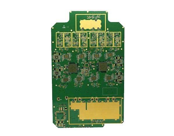
Digital high speed pcb application
Optimizing Signal Integrity in High-Speed PCB Design
In the realm of digital high-speed printed circuit board (PCB) design, optimizing signal integrity is paramount to ensuring the reliable performance of electronic systems. As data rates continue to escalate, the challenges associated with maintaining signal integrity become increasingly complex. Consequently, designers must employ a variety of strategies to mitigate issues such as signal degradation, crosstalk, and electromagnetic interference (EMI).
One of the fundamental aspects of optimizing signal integrity in high-speed PCB design is the careful consideration of trace geometry.
The width, length, and spacing of traces can significantly impact signal quality. For instance, impedance control is crucial; mismatched impedance can lead to signal reflections, which degrade the signal quality. To achieve controlled impedance, designers often use differential pairs and carefully calculate the trace dimensions and the dielectric properties of the PCB material. Additionally, maintaining consistent trace width and spacing helps to minimize variations in impedance, further enhancing signal integrity.
Transitioning to another critical factor, the layout of the PCB plays a vital role in signal integrity.
Proper component placement and routing are essential to minimize signal path lengths and reduce the potential for crosstalk. Placing high-speed components close to each other and routing high-speed signals on inner layers, sandwiched between ground planes, can significantly reduce EMI. Moreover, the use of ground planes not only provides a return path for signals but also helps to shield sensitive traces from external noise sources.
Furthermore, the choice of materials in PCB fabrication can influence signal integrity.
High-frequency signals are more susceptible to losses due to the dielectric properties of the PCB substrate. Materials with low dielectric constant (Dk) and low dissipation factor (Df) are preferred for high-speed applications as they exhibit lower signal attenuation and dispersion. Advanced materials such as polytetrafluoroethylene (PTFE) and other high-performance laminates are often employed in high-speed PCB designs to ensure minimal signal loss.
In addition to material selection, the implementation of proper termination techniques is essential to prevent signal reflections.
Termination resistors, either series or parallel, can be used to match the impedance of the transmission line to the load, thereby minimizing reflections. Series termination is often used in point-to-point connections, while parallel termination is more suitable for multi-drop bus systems. The correct application of these techniques ensures that signals are transmitted cleanly and without distortion.
Moreover, power integrity is intrinsically linked to signal integrity in high-speed PCB design.
Fluctuations in power supply can introduce noise into the signal paths, adversely affecting signal quality. To mitigate this, designers employ decoupling capacitors strategically placed near power pins of integrated circuits (ICs) to filter out high-frequency noise. Additionally, the use of power and ground planes with low inductance paths helps to maintain a stable power supply, further enhancing signal integrity.
Lastly, simulation and modeling tools are indispensable in the design process for optimizing signal integrity.
These tools allow designers to predict and analyze the behavior of high-speed signals within the PCB, identifying potential issues before physical prototyping. By simulating various scenarios, designers can make informed decisions about trace routing, impedance control, and termination strategies, ultimately leading to a more robust design.
In conclusion, optimizing signal integrity in high-speed PCB design is a multifaceted challenge that requires careful consideration of trace geometry, layout, material selection, termination techniques, and power integrity. By employing these strategies and leveraging advanced simulation tools, designers can ensure that their high-speed digital systems perform reliably and efficiently in increasingly demanding applications.
Techniques for Reducing Electromagnetic Interference in High-Speed PCBs
In the realm of digital high-speed printed circuit boards (PCBs), managing electromagnetic interference (EMI) is paramount to ensuring optimal performance and reliability. As the demand for faster data transmission rates continues to escalate, the susceptibility of high-speed PCBs to EMI becomes a critical concern. Consequently, engineers must employ a variety of techniques to mitigate these unwanted electromagnetic emissions and maintain signal integrity.
One fundamental approach to reducing EMI in high-speed PCBs is through meticulous layout design.
Proper component placement and routing are essential to minimize the loop areas that can act as antennas, radiating unwanted electromagnetic waves. By strategically positioning high-speed components and ensuring that signal traces are as short and direct as possible, engineers can significantly reduce the potential for EMI. Additionally, maintaining a consistent ground plane beneath signal traces helps to provide a low-impedance return path, further mitigating EMI.
Another effective technique involves the use of differential signaling.
Differential pairs, which consist of two complementary signals, are less susceptible to external noise and generate lower levels of EMI compared to single-ended signals. This is because the electromagnetic fields generated by the two signals tend to cancel each other out, resulting in reduced radiation. Moreover, differential signaling enhances signal integrity by providing better noise immunity, making it a preferred choice for high-speed data transmission.
Shielding is also a crucial method for EMI reduction in high-speed PCBs.
By enclosing sensitive components and traces within conductive enclosures or using shielded cables, engineers can prevent external electromagnetic fields from interfering with the PCB’s operation. This technique is particularly effective in environments with high levels of ambient EMI, such as industrial settings or areas with numerous electronic devices. Additionally, implementing ground stitching vias around the periphery of the PCB can help to create a Faraday cage effect, further enhancing the shielding effectiveness.
The use of decoupling capacitors is another vital strategy for mitigating EMI.
These capacitors are placed close to power supply pins of integrated circuits to filter out high-frequency noise and provide a stable power supply. By selecting capacitors with appropriate values and placing them strategically, engineers can effectively suppress power supply noise, which is a common source of EMI in high-speed PCBs. Furthermore, employing a combination of capacitors with different values can provide a broader frequency range of noise suppression.
In addition to these techniques, careful consideration of the PCB’s stack-up configuration can play a significant role in EMI reduction.
A well-designed stack-up with alternating signal and ground layers can help to contain electromagnetic fields within the PCB, reducing radiation and crosstalk between adjacent traces. This configuration also enhances the overall signal integrity by providing controlled impedance and minimizing signal reflections.
Lastly, the implementation of proper termination techniques is essential for minimizing EMI in high-speed PCBs.
Impedance mismatches at the ends of signal traces can lead to signal reflections, which not only degrade signal quality but also contribute to EMI. By using appropriate termination resistors and ensuring that the impedance of the traces matches the source and load, engineers can effectively reduce reflections and their associated electromagnetic emissions.
In conclusion, reducing electromagnetic interference in high-speed PCBs requires a multifaceted approach that encompasses careful layout design, differential signaling, shielding, decoupling capacitors, stack-up configuration, and proper termination techniques. By employing these strategies, engineers can enhance the performance and reliability of high-speed digital PCBs, ensuring that they meet the stringent demands of modern electronic applications.
Material Selection for High-Frequency PCB Applications
In the realm of high-frequency printed circuit boards (PCBs), material selection is a critical factor that significantly influences the performance and reliability of the final product. As digital systems continue to evolve, the demand for high-speed data transmission has surged, necessitating the use of materials that can support these advanced requirements. Consequently, understanding the properties and implications of various materials is essential for engineers and designers working on high-frequency PCB applications.
To begin with, one of the primary considerations in material selection is the dielectric constant (Dk).
The dielectric constant affects the signal propagation speed and impedance of the PCB. Materials with a low and stable dielectric constant are preferred for high-frequency applications because they minimize signal loss and ensure consistent performance across a range of frequencies. For instance, polytetrafluoroethylene (PTFE), commonly known as Teflon, is widely used due to its low Dk and excellent electrical properties. However, PTFE can be challenging to process and is often more expensive than other materials.
In addition to the dielectric constant, the dissipation factor (Df) is another crucial parameter.
The dissipation factor measures the energy loss as heat within the dielectric material. A low dissipation factor is desirable for high-frequency PCBs as it reduces signal attenuation and power loss. Materials such as Rogers RO3000 and RO4000 series are known for their low Df, making them suitable for applications requiring minimal signal degradation.
Thermal management is also a significant concern in high-frequency PCB design.
As operating frequencies increase, so does the heat generated by the components. Therefore, materials with good thermal conductivity are essential to dissipate heat effectively and maintain the integrity of the PCB. Ceramic-filled laminates, for example, offer excellent thermal performance and are often used in high-power applications. Additionally, materials like FR-4, which is a glass-reinforced epoxy laminate, are commonly used due to their balance of cost, mechanical strength, and thermal properties. However, FR-4 may not always be suitable for very high-frequency applications due to its higher Dk and Df compared to specialized materials.
Moreover, the coefficient of thermal expansion (CTE) is a vital factor to consider.
The CTE measures how much a material expands or contracts with temperature changes. A low and matched CTE between the PCB material and the components is crucial to prevent mechanical stress and potential failure during thermal cycling. Materials such as polyimide and certain ceramic-filled substrates exhibit low CTE, making them ideal for high-reliability applications where thermal stability is paramount.
Furthermore, signal integrity is a key aspect that can be influenced by the choice of PCB material.
High-frequency signals are susceptible to various forms of interference and loss, including crosstalk, reflection, and electromagnetic interference (EMI). Selecting materials with low loss tangents and high-quality copper foils can mitigate these issues, ensuring cleaner signal transmission. Advanced materials like liquid crystal polymer (LCP) and certain high-performance thermoset resins are engineered to provide superior signal integrity for high-speed digital applications.
In conclusion, the selection of materials for high-frequency PCB applications is a multifaceted process that requires careful consideration of various electrical, thermal, and mechanical properties. By understanding the implications of dielectric constant, dissipation factor, thermal conductivity, coefficient of thermal expansion, and signal integrity, engineers can make informed decisions that enhance the performance and reliability of high-speed digital systems. As technology continues to advance, the development and utilization of specialized materials will remain a cornerstone in the pursuit of optimal high-frequency PCB designs.
Advanced Routing Strategies for High-Speed Digital Circuits
In the realm of high-speed digital circuits, the importance of advanced routing strategies cannot be overstated. As the demand for faster data transmission and higher processing speeds continues to escalate, the design and implementation of printed circuit boards (PCBs) must evolve to meet these rigorous requirements.
One of the primary challenges in high-speed digital PCB design is managing signal integrity, which is crucial for ensuring reliable and efficient performance.
To address this, engineers employ a variety of advanced routing techniques that mitigate issues such as signal reflection, crosstalk, and electromagnetic interference (EMI).
Firstly, controlled impedance routing is a fundamental strategy in high-speed PCB design.
This technique involves designing traces with specific widths and spacing to maintain a consistent impedance, which is essential for minimizing signal reflections. By carefully controlling the impedance, designers can ensure that signals travel smoothly along the traces without significant degradation. This is particularly important for differential pairs, where maintaining a consistent impedance between the two traces is critical for preserving signal integrity.
In addition to controlled impedance, the use of differential signaling is another key strategy.
Differential pairs consist of two traces that carry equal and opposite signals. This configuration helps to cancel out noise and reduce EMI, as any external interference affects both traces equally and is subsequently negated. Differential signaling is especially beneficial in high-speed applications where signal integrity is paramount, such as in data communication and high-frequency clock distribution.
Another advanced routing strategy is the implementation of via stitching and ground planes.
Via stitching involves placing multiple vias around high-speed signal traces to connect different layers of the PCB, thereby providing a low-impedance path for return currents. This technique helps to reduce EMI and improve signal integrity by ensuring that return currents follow a predictable path. Ground planes, on the other hand, provide a continuous reference plane for high-speed signals, further enhancing signal integrity and reducing noise.
Moreover, the use of serpentine routing is a technique employed to match the lengths of differential pairs or other critical signal paths.
In high-speed digital circuits, even slight differences in trace lengths can lead to timing mismatches and signal skew. Serpentine routing involves creating meandering patterns in the traces to equalize their lengths, ensuring that signals arrive at their destination simultaneously. This is particularly important in applications such as memory interfaces and high-speed data buses, where precise timing is crucial.
Furthermore, the strategic placement of decoupling capacitors is essential for maintaining power integrity in high-speed digital circuits.
Decoupling capacitors help to filter out noise and provide a stable power supply to the components. By placing these capacitors close to the power pins of integrated circuits, designers can minimize voltage fluctuations and ensure reliable operation. This practice is especially important in high-speed designs, where even minor power supply variations can lead to significant performance issues.
Lastly, signal layer stacking and careful layer management play a critical role in high-speed PCB design.
By strategically arranging signal, power, and ground layers, designers can minimize crosstalk and EMI while optimizing signal integrity. For instance, placing ground planes adjacent to signal layers helps to shield the signals from external interference and provides a low-impedance return path for high-speed currents.
In conclusion, advanced routing strategies are indispensable for the successful design and implementation of high-speed digital circuits. Techniques such as controlled impedance routing, differential signaling, via stitching, serpentine routing, strategic decoupling capacitor placement, and careful layer management collectively contribute to maintaining signal integrity, reducing EMI, and ensuring reliable performance. As the demand for higher speeds and greater data throughput continues to grow, the adoption of these advanced routing strategies will remain a cornerstone of high-speed PCB design.