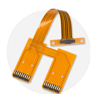
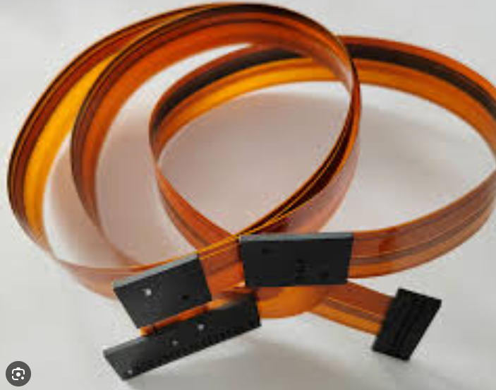
Flex pcb fpc
Advantages Of Using Flex PCB In Modern Electronics
Flex PCBs, or flexible printed circuit boards, have become increasingly prevalent in modern electronics due to their numerous advantages over traditional rigid PCBs.
One of the primary benefits of flex PCBs is their ability to bend and conform to various shapes and spaces, which allows for greater design flexibility.
This adaptability is particularly valuable in applications where space is limited or where the electronic components need to fit into unconventional shapes. For instance, in wearable technology, medical devices, and compact consumer electronics, the ability to mold the circuit board to the device’s form factor is crucial.
Moreover, flex PCBs contribute to the reduction of weight and volume in electronic devices
Traditional rigid PCBs can be bulky and heavy, which is a significant drawback in portable and handheld devices. Flex PCBs, on the other hand, are made from lightweight materials such as polyimide, which not only reduces the overall weight of the device but also enhances its portability. This weight reduction is particularly beneficial in aerospace and automotive industries, where every gram counts towards improving fuel efficiency and performance.
In addition to their physical flexibility and lightweight nature, flex PCBs offer improved reliability and durability.
The materials used in flex PCBs are designed to withstand harsh environments, including extreme temperatures, vibrations, and mechanical stresses. This makes them ideal for use in industrial applications and other demanding environments where traditional rigid PCBs might fail. Furthermore, the inherent flexibility of these boards allows them to absorb shocks and vibrations better, reducing the risk of damage and increasing the lifespan of the electronic device.
Another significant advantage of flex PCBs is their ability to simplify complex interconnections.
In traditional rigid PCB assemblies, multiple boards and connectors are often required to achieve the desired functionality, which can lead to increased complexity and potential points of failure. Flex PCBs can integrate multiple layers and components into a single, continuous circuit, reducing the need for additional connectors and simplifying the overall design. This not only enhances the reliability of the device but also streamlines the manufacturing process, leading to cost savings and faster production times.
Furthermore, flex PCBs offer enhanced signal integrity and performance.
The materials used in flex PCBs have excellent electrical properties, which help to minimize signal loss and interference. This is particularly important in high-frequency applications, where maintaining signal integrity is critical. Additionally, the ability to design complex, three-dimensional circuits with flex PCBs allows for shorter signal paths, further reducing the potential for signal degradation.
The environmental benefits of flex PCBs should not be overlooked either.
The manufacturing process for flex PCBs typically generates less waste compared to traditional rigid PCBs. The use of flexible materials also means that fewer raw materials are required, contributing to a reduction in the overall environmental footprint of electronic devices. As sustainability becomes an increasingly important consideration in the electronics industry, the adoption of flex PCBs can play a role in promoting more eco-friendly manufacturing practices.
In conclusion, the advantages of using flex PCBs in modern electronics are manifold. Their ability to conform to various shapes and spaces, reduce weight and volume, improve reliability and durability, simplify complex interconnections, enhance signal integrity, and offer environmental benefits make them an attractive choice for a wide range of applications. As technology continues to evolve, the demand for flexible, efficient, and reliable electronic components will only grow, further solidifying the importance of flex PCBs in the future of electronics.
Design Tips For Creating Reliable Flex PCBs
When designing flexible printed circuit boards (FPCs), it is crucial to consider several factors to ensure reliability and performance.
Flex PCBs offer numerous advantages, such as reduced weight, space savings, and the ability to conform to complex geometries. However, their unique characteristics necessitate careful planning and execution during the design phase. To begin with, understanding the material properties is essential. Flex PCBs are typically made from polyimide, a material known for its excellent thermal stability and mechanical flexibility. Selecting the appropriate thickness of the polyimide substrate is vital, as it directly impacts the board’s flexibility and durability. Thinner substrates offer greater flexibility but may be more prone to mechanical damage, while thicker substrates provide enhanced durability at the cost of reduced flexibility.
Transitioning to the layout design, it is important to minimize stress points.
Sharp corners and abrupt changes in trace direction can create stress concentrations, leading to potential failures. Instead, designers should use curved traces and gradual transitions to distribute mechanical stress more evenly. Additionally, maintaining a consistent trace width and spacing helps to avoid localized stress and ensures uniform current distribution. Another critical aspect is the bend radius. Flex PCBs are often subjected to bending and flexing during installation and operation. Adhering to the recommended minimum bend radius, typically specified by the material manufacturer, is essential to prevent cracking and delamination. A general rule of thumb is to maintain a bend radius of at least ten times the thickness of the flex PCB.
Furthermore, the placement of components and vias requires careful consideration.
Placing components too close to bend areas can lead to mechanical stress and potential failure. It is advisable to keep components and vias away from high-stress regions and to use teardrop-shaped pads to reduce stress concentrations around vias. Additionally, reinforcing critical areas with stiffeners can provide extra support and prevent damage during bending. Moving on to the electrical design, signal integrity is a key concern. Flex PCBs can exhibit higher levels of electromagnetic interference (EMI) due to their thin and flexible nature. To mitigate EMI, designers should use ground planes and shielding techniques. Ensuring proper grounding and minimizing the loop area of signal traces can significantly reduce EMI and improve signal integrity.
Thermal management is another important consideration.
Flex PCBs can experience significant temperature variations during operation, which can affect their performance and longevity. Using thermal vias and heat sinks can help dissipate heat effectively. Additionally, selecting materials with good thermal conductivity and ensuring proper ventilation can further enhance thermal management. In terms of manufacturing, working closely with the PCB manufacturer from the early stages of design can help identify potential issues and optimize the design for manufacturability. Manufacturers can provide valuable insights into material selection, layer stack-up, and fabrication processes, ensuring that the final product meets the desired specifications.
Lastly, thorough testing and validation are essential to ensure the reliability of flex PCBs.
Conducting mechanical stress tests, thermal cycling tests, and electrical performance tests can help identify potential weaknesses and validate the design under real-world conditions. Incorporating these design tips can significantly enhance the reliability and performance of flex PCBs, ensuring they meet the demands of modern electronic applications. By carefully considering material properties, layout design, component placement, signal integrity, thermal management, and manufacturing processes, designers can create robust and reliable flex PCBs that deliver optimal performance in a wide range of applications.
Common Applications Of Flexible Printed Circuits
Flexible printed circuits (FPCs), commonly referred to as flex PCBs, have become integral components in a wide array of modern electronic devices. Their unique ability to bend, fold, and conform to various shapes and spaces makes them indispensable in applications where traditional rigid PCBs would be impractical or impossible to use. As technology continues to advance, the demand for more compact, lightweight, and versatile electronic solutions has driven the proliferation of FPCs across numerous industries.
One of the most prevalent applications of flexible printed circuits is in the consumer electronics sector.
Devices such as smartphones, tablets, and wearable technology rely heavily on FPCs to achieve their sleek, compact designs. The flexibility of these circuits allows for the integration of multiple functions within a limited space, enhancing the overall performance and user experience. For instance, in smartphones, FPCs are used to connect various components such as the display, camera, and battery, enabling the device to maintain its slim profile while ensuring robust functionality.
In addition to consumer electronics, the automotive industry has also embraced the advantages of flexible printed circuits.
Modern vehicles are equipped with an increasing number of electronic systems, including advanced driver-assistance systems (ADAS), infotainment systems, and various sensors. FPCs are utilized in these applications to reduce weight, improve reliability, and enhance the overall efficiency of the vehicle’s electronic architecture. By replacing traditional wiring harnesses with flexible circuits, manufacturers can achieve significant space savings and reduce the complexity of the assembly process.
The medical field is another area where flexible printed circuits have made a substantial impact.
Medical devices such as pacemakers, hearing aids, and diagnostic equipment benefit from the miniaturization and flexibility offered by FPCs. These circuits enable the development of smaller, more comfortable, and less invasive devices, which can lead to improved patient outcomes. For example, in wearable medical devices, FPCs allow for continuous monitoring of vital signs without causing discomfort to the patient, thereby facilitating better long-term health management.
Moreover, the aerospace and defense industries have recognized the potential of flexible printed circuits in enhancing the performance and reliability of their systems.
In aerospace applications, where weight and space are critical considerations, FPCs provide a lightweight and compact solution for connecting various electronic components. This is particularly important in satellites, unmanned aerial vehicles (UAVs), and other space-constrained environments. Similarly, in defense applications, the durability and flexibility of FPCs make them suitable for use in rugged and demanding conditions, ensuring the reliability of mission-critical systems.
Furthermore, the industrial sector has also seen significant benefits from the adoption of flexible printed circuits.
Industrial automation and robotics often require complex and dynamic movements, which can be challenging to achieve with rigid PCBs. FPCs offer the necessary flexibility to accommodate these movements, enabling the development of more efficient and reliable automated systems. Additionally, the ability to withstand harsh environmental conditions makes FPCs ideal for use in industrial applications where exposure to extreme temperatures, chemicals, and mechanical stress is common.
In conclusion, the versatility and adaptability of flexible printed circuits have led to their widespread adoption across various industries. From consumer electronics to automotive, medical, aerospace, defense, and industrial applications, FPCs have proven to be a critical component in the advancement of modern technology. As the demand for more compact, lightweight, and efficient electronic solutions continues to grow, the role of flexible printed circuits is expected to expand even further, driving innovation and enabling new possibilities in the world of electronics.
Manufacturing Process Of Flex PCBs: A Step-By-Step Guide
The manufacturing process of Flex PCBs (Flexible Printed Circuit Boards) is a meticulous and intricate procedure that demands precision and expertise. Flex PCBs, also known as FPCs (Flexible Printed Circuits), are essential components in modern electronics due to their ability to bend and conform to various shapes, making them ideal for compact and complex devices. The journey from raw materials to a fully functional Flex PCB involves several critical steps, each contributing to the final product’s reliability and performance.
To begin with, the process starts with the selection of the base material, typically a flexible polymer such as polyimide.
This material is chosen for its excellent thermal stability and flexibility. The polyimide film is then coated with a thin layer of copper, which serves as the conductive material. This copper-clad laminate forms the foundation upon which the circuit will be built.
Following the preparation of the base material, the next step is the application of a photoresist.
This light-sensitive material is applied to the copper surface and then exposed to ultraviolet (UV) light through a photomask. The photomask contains the desired circuit pattern, and the UV exposure hardens the photoresist in the areas where the circuit paths are to be formed. Subsequently, the unexposed photoresist is removed, revealing the copper that needs to be etched away.
The etching process involves immersing the laminate in a chemical solution that dissolves the exposed copper, leaving behind the desired circuit pattern protected by the hardened photoresist. After etching, the remaining photoresist is stripped away, exposing the clean copper circuit paths. At this stage, the Flex PCB begins to take shape, but it is still far from complete.
To ensure the circuit’s durability and reliability, a protective layer known as a coverlay is applied. The coverlay, typically made of polyimide or a similar material, is laminated over the circuit to shield it from environmental factors such as moisture, dust, and mechanical stress. Openings are created in the coverlay to allow for soldering and electrical connections.
Next, the process moves to the drilling stage, where precise holes, or vias, are drilled into the PCB. These vias enable electrical connections between different layers of the circuit. Advanced drilling techniques, such as laser drilling, are often employed to achieve the high precision required for modern Flex PCBs.
Following drilling, the vias are plated with copper to establish electrical continuity between the layers.
This step is crucial for the functionality of multi-layer Flex PCBs, which are common in complex electronic devices. The copper plating process involves electroplating, where the PCB is immersed in a copper sulfate solution and an electric current is applied to deposit copper onto the vias’ walls.
Once the vias are plated, the Flex PCB undergoes a series of inspections and tests to ensure its quality and functionality. These tests include electrical testing to verify the continuity and integrity of the circuit paths, as well as visual inspections to detect any defects or irregularities.
Finally, the Flex PCB is cut to its final shape and size, and any additional components, such as connectors or stiffeners, are added. The completed Flex PCB is then ready for integration into electronic devices, where its flexibility and reliability will contribute to the overall performance and functionality of the end product.
In conclusion, the manufacturing process of Flex PCBs is a complex and precise procedure that involves multiple steps, from material selection to final inspection. Each stage is critical to ensuring the quality and performance of the final product, making Flex PCBs indispensable in the ever-evolving world of electronics.