Multilayer pcb technology
Advantages Of Multilayer PCB Technology
Multilayer PCB technology has revolutionized the electronics industry, offering numerous advantages that have made it the preferred choice for a wide range of applications.
One of the primary benefits of multilayer PCBs is their ability to support higher component density.
By stacking multiple layers of circuitry within a single board, designers can create more complex and compact electronic devices. This increased density is particularly advantageous in modern electronics, where space is often at a premium, and the demand for miniaturization continues to grow.
In addition to supporting higher component density, multilayer PCBs also enhance electrical performance.
The close proximity of the layers allows for shorter signal paths, which in turn reduces signal loss and improves overall signal integrity. This is especially critical in high-frequency applications, where even minor signal degradation can lead to significant performance issues. Furthermore, the ability to incorporate ground and power planes within the layers helps to minimize electromagnetic interference (EMI) and crosstalk, ensuring that the device operates reliably and efficiently.
Another significant advantage of multilayer PCB technology is its contribution to improved thermal management.
As electronic devices become more powerful, they generate more heat, which can adversely affect performance and longevity. Multilayer PCBs can be designed with dedicated thermal vias and heat sinks to effectively dissipate heat away from critical components. This enhanced thermal management capability not only helps to maintain optimal operating temperatures but also extends the lifespan of the device.
Moreover, multilayer PCBs offer greater design flexibility compared to their single-layer counterparts.
The ability to route complex circuits across multiple layers allows designers to optimize the layout for both performance and manufacturability. This flexibility is particularly beneficial in applications that require intricate circuitry, such as advanced communication systems, medical devices, and aerospace technology. By leveraging the advantages of multilayer PCBs, designers can achieve the desired functionality without compromising on size or performance.
The reliability of multilayer PCBs is another noteworthy advantage.
The use of multiple layers provides redundancy, which can be crucial in mission-critical applications. For instance, if one layer experiences a failure, the other layers can continue to function, thereby preventing a complete system shutdown. Additionally, the robust construction of multilayer PCBs, which often includes advanced materials and manufacturing techniques, ensures that they can withstand harsh environmental conditions and mechanical stress.
Cost-effectiveness is also a key consideration when evaluating the advantages of multilayer PCB technology
. While the initial design and manufacturing costs may be higher compared to single-layer PCBs, the long-term benefits often outweigh these expenses. The increased functionality, improved performance, and enhanced reliability of multilayer PCBs can lead to reduced maintenance costs and fewer failures over the device’s lifespan. Furthermore, the ability to integrate more components into a smaller footprint can result in cost savings in terms of materials and assembly.
In conclusion, multilayer PCB technology offers a multitude of advantages that make it an indispensable component in modern electronics. From supporting higher component density and enhancing electrical performance to improving thermal management and providing greater design flexibility, multilayer PCBs address many of the challenges faced by today’s electronic devices. Their reliability and cost-effectiveness further underscore their value, making them a preferred choice for a wide range of applications. As technology continues to advance, the role of multilayer PCBs in enabling innovation and driving progress will undoubtedly remain significant.
Design Considerations For Multilayer PCBs
Multilayer PCB technology has revolutionized the electronics industry by enabling the design and manufacture of complex, high-performance electronic devices. When designing multilayer PCBs, several critical considerations must be taken into account to ensure optimal functionality, reliability, and manufacturability.
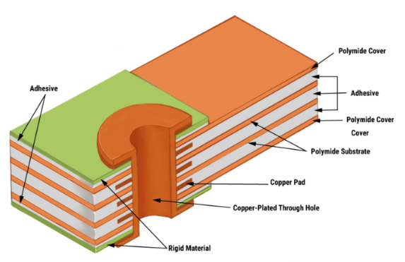
One of the primary factors to consider is the layer stack-up configuration.
The arrangement of signal, power, and ground layers within the PCB stack-up significantly impacts the board’s electrical performance. Proper layer stack-up can minimize electromagnetic interference (EMI) and crosstalk, which are crucial for maintaining signal integrity in high-speed circuits. Typically, designers use alternating layers of signal and ground planes to provide effective shielding and return paths for signals.
Another essential consideration is the selection of materials.
The choice of substrate material affects the PCB’s thermal and electrical properties. High-frequency applications often require materials with low dielectric constant and low loss tangent to reduce signal attenuation and dispersion. Additionally, thermal management is a critical aspect, especially for high-power applications. Materials with high thermal conductivity can help dissipate heat more effectively, thereby enhancing the reliability and longevity of the PCB.
Furthermore, via design plays a pivotal role in multilayer PCBs.
Vias are used to establish electrical connections between different layers. There are various types of vias, including through-hole vias, blind vias, and buried vias. Each type has its advantages and limitations. For instance, blind and buried vias can save space on the outer layers, allowing for more compact designs. However, they are more complex and costly to manufacture compared to through-hole vias. Therefore, designers must carefully evaluate the trade-offs between space savings and manufacturing complexity.
Signal integrity is another critical aspect that must be addressed during the design phase.
High-speed signals are susceptible to various forms of degradation, such as reflection, attenuation, and crosstalk. To mitigate these issues, designers often employ techniques such as controlled impedance routing, differential pair routing, and proper termination. Controlled impedance routing ensures that the impedance of the signal traces matches the characteristic impedance of the transmission line, thereby minimizing reflections. Differential pair routing helps reduce noise and EMI by using two complementary signals that cancel each other out.
Power integrity is equally important in multilayer PCB design.
Ensuring a stable power supply to all components is crucial for the reliable operation of the circuit. Designers must pay attention to the layout of power and ground planes to minimize voltage drops and noise. Decoupling capacitors are commonly used to filter out high-frequency noise and provide a stable power supply to the components. The placement and value of these capacitors must be carefully chosen to achieve optimal performance.
Thermal management is another vital consideration, particularly for high-power applications.
Excessive heat can lead to component failure and reduced lifespan of the PCB. Designers must incorporate adequate thermal vias, heat sinks, and thermal pads to dissipate heat effectively. Additionally, the layout should be optimized to ensure even heat distribution across the board.
In conclusion, designing multilayer PCBs involves a complex interplay of various factors, including layer stack-up configuration, material selection, via design, signal integrity, power integrity, and thermal management. Each of these considerations plays a crucial role in ensuring the optimal performance, reliability, and manufacturability of the final product. By carefully addressing these aspects, designers can create high-performance multilayer PCBs that meet the stringent requirements of modern electronic devices.
Applications Of Multilayer PCBs In Modern Electronics
Multilayer PCB technology has become a cornerstone in the development of modern electronics, offering unparalleled advantages in terms of design flexibility, performance, and miniaturization. As electronic devices continue to evolve, the demand for more complex and compact circuitry has driven the widespread adoption of multilayer printed circuit boards (PCBs). These advanced PCBs consist of multiple layers of conductive material separated by insulating layers, allowing for intricate and high-density circuit designs that are essential for contemporary electronic applications.
One of the primary applications of multilayer PCBs is in the realm of consumer electronics.
Smartphones, tablets, and laptops are quintessential examples of devices that benefit immensely from this technology. The compact nature of multilayer PCBs enables manufacturers to pack more functionality into smaller form factors, which is crucial for portable devices. Additionally, the enhanced electrical performance provided by these PCBs ensures that high-speed data transmission and signal integrity are maintained, which is vital for the seamless operation of modern gadgets.
Transitioning to the automotive industry, multilayer PCBs play a pivotal role in the development of advanced vehicular systems.
Modern automobiles are equipped with a plethora of electronic components, ranging from engine control units (ECUs) to advanced driver-assistance systems (ADAS). The complexity and reliability required for these systems necessitate the use of multilayer PCBs. For instance, ECUs rely on these PCBs to manage engine performance, emissions, and fuel efficiency, while ADAS systems depend on them for processing data from various sensors to enhance vehicle safety and automation.
In the field of telecommunications, multilayer PCBs are indispensable for the infrastructure that supports global connectivity.
Base stations, routers, and switches all utilize these advanced PCBs to handle the high-frequency signals and large volumes of data that are characteristic of modern communication networks. The ability of multilayer PCBs to support high-speed signal transmission and reduce electromagnetic interference (EMI) is crucial for maintaining the integrity and efficiency of telecommunication systems.
Moreover, the medical industry has also seen significant advancements due to the integration of multilayer PCB technology.
Medical devices such as MRI machines, pacemakers, and diagnostic equipment require highly reliable and precise electronic components. Multilayer PCBs provide the necessary reliability and miniaturization, enabling the development of compact and sophisticated medical devices that can perform complex functions with high accuracy. This technology not only enhances the functionality of medical equipment but also contributes to improved patient outcomes through more accurate diagnostics and effective treatments.
Furthermore, the aerospace and defense sectors have long been proponents of multilayer PCB technology due to its robustness and reliability.
In these industries, electronic systems must withstand extreme conditions, including high temperatures, vibrations, and radiation. Multilayer PCBs are designed to meet these stringent requirements, making them ideal for applications such as satellite communications, radar systems, and avionics. The ability to integrate multiple functions into a single, compact PCB also helps in reducing the weight and space constraints that are critical in aerospace applications.
In conclusion, the applications of multilayer PCBs in modern electronics are vast and varied, spanning across multiple industries including consumer electronics, automotive, telecommunications, medical, and aerospace. The technology’s ability to support complex, high-density circuit designs while maintaining reliability and performance makes it an essential component in the advancement of contemporary electronic devices. As the demand for more sophisticated and compact electronics continues to grow, the role of multilayer PCBs will undoubtedly become even more significant, driving innovation and progress in various fields.
Manufacturing Process Of Multilayer PCBs
The manufacturing process of multilayer printed circuit boards (PCBs) is a sophisticated and intricate procedure that demands precision and expertise. It begins with the design phase, where engineers use advanced software to create a detailed blueprint of the PCB. This blueprint includes the layout of the various layers, the placement of components, and the routing of electrical connections. Once the design is finalized, it is converted into a format that can be used by the manufacturing equipment.
The first step in the actual manufacturing process is the creation of the individual layers.
Each layer is made from a thin sheet of insulating material, typically fiberglass, coated with a layer of copper. The copper is then etched away using a chemical process to create the desired circuit pattern. This is done for each layer separately, ensuring that the intricate designs are accurately replicated.
Following the etching process, the layers are aligned and laminated together under high pressure and temperature.
This step is crucial as it ensures that the layers are perfectly aligned and securely bonded. Misalignment at this stage can lead to electrical failures and reduced performance of the final product. The laminated board is then drilled to create holes for the electrical connections between the layers. These holes, known as vias, are plated with copper to establish a conductive path.
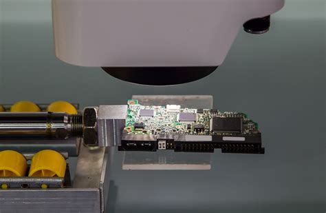
Subsequently, the board undergoes a series of inspections and tests to ensure that it meets the required specifications.
Optical inspection systems are used to check for any defects in the circuit patterns, while electrical tests verify the continuity and integrity of the connections. Any defects identified at this stage are rectified to prevent issues in the final product.
Once the board passes these inspections, it moves on to the solder mask application. The solder mask is a protective layer that prevents solder from bridging between conductive traces and causing short circuits. It also provides a surface for the application of the silkscreen, which is used to print labels and component identifiers on the board. The solder mask is applied using a photolithographic process, which ensures precise coverage and alignment.
Following the application of the solder mask, the board is subjected to surface finish processes.
These processes involve coating the exposed copper areas with a protective layer to prevent oxidation and ensure good solderability. Common surface finishes include HASL (Hot Air Solder Leveling), ENIG (Electroless Nickel Immersion Gold), and OSP (Organic Solderability Preservative). Each finish has its own advantages and is chosen based on the specific requirements of the application.
The final step in the manufacturing process is the assembly of the components onto the PCB.
This is typically done using automated pick-and-place machines, which accurately position and solder the components onto the board. The assembled board is then subjected to a series of functional tests to ensure that it operates as intended. These tests may include in-circuit testing, functional testing, and burn-in testing, depending on the complexity and criticality of the application.
In conclusion, the manufacturing process of multilayer PCBs is a complex and meticulous procedure that involves multiple stages, each requiring a high degree of precision and control. From the initial design phase to the final assembly and testing, every step is crucial in ensuring the reliability and performance of the final product. As technology continues to advance, the processes and techniques used in PCB manufacturing are continually evolving, enabling the production of increasingly sophisticated and high-performance electronic devices.