Radio frequency printed circuit boards
Introduction To Radio Frequency Printed Circuit Boards
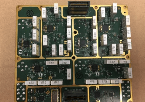
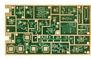
Radio frequency printed circuit boards (RF PCBs) are specialized types of PCBs designed to operate at high frequencies, typically in the range of megahertz (MHz) to gigahertz (GHz). These boards are integral to the functionality of various high-frequency applications, including wireless communication systems, radar systems, and satellite communications.
Understanding the unique characteristics and design considerations of RF PCBs is essential for engineers and designers working in these advanced technological fields.
To begin with, RF PCBs differ significantly from standard PCBs due to the high-frequency signals they must handle.
At these elevated frequencies, even minor imperfections in the PCB design can lead to significant signal loss or interference. Therefore, the materials used in RF PCBs are chosen for their superior electrical properties, such as low dielectric constant and low loss tangent. Common materials include PTFE (polytetrafluoroethylene), ceramic-filled PTFE, and other high-performance laminates. These materials help to minimize signal attenuation and ensure the integrity of the transmitted signals.
Moreover, the layout and design of RF PCBs require meticulous attention to detail.
Signal integrity is paramount, and designers must consider factors such as trace width, spacing, and the use of ground planes to reduce electromagnetic interference (EMI). The impedance of the transmission lines must be carefully controlled to match the characteristic impedance of the connected components, thereby minimizing reflections and signal loss. Additionally, the use of via structures and the placement of components must be optimized to prevent unwanted parasitic effects that could degrade performance.
Transitioning to the manufacturing process, RF PCBs present unique challenges that necessitate specialized fabrication techniques.
The precision required in etching fine traces and maintaining tight tolerances is higher than that for conventional PCBs. Advanced photolithography and etching processes are employed to achieve the necessary accuracy. Furthermore, the choice of solder mask and surface finish is critical, as these can impact the board’s high-frequency performance. For instance, the use of ENIG (Electroless Nickel Immersion Gold) or immersion silver finishes can provide better signal integrity compared to traditional HASL (Hot Air Solder Leveling) finishes.
In addition to the technical aspects, the testing and validation of RF PCBs are equally crucial.
High-frequency testing equipment, such as network analyzers and spectrum analyzers, is used to measure parameters like return loss, insertion loss, and signal integrity. These tests ensure that the RF PCB meets the stringent performance criteria required for its intended application. Any deviations from the expected performance can lead to costly redesigns and delays in product development.
Furthermore, the integration of RF PCBs into larger systems necessitates careful consideration of thermal management.
High-frequency components can generate significant heat, which must be dissipated effectively to maintain reliable operation. Thermal vias, heat sinks, and advanced cooling techniques are often employed to manage the thermal load and prevent overheating.
In conclusion, radio frequency printed circuit boards are a critical component in the realm of high-frequency electronics. Their design, material selection, manufacturing, and testing require a high level of expertise and precision. As technology continues to advance and the demand for high-frequency applications grows, the importance of RF PCBs will only increase. Engineers and designers must stay abreast of the latest developments in materials, fabrication techniques, and testing methodologies to ensure the successful implementation of RF PCBs in cutting-edge technologies.
Design Considerations For RF PCBs
Designing radio frequency (RF) printed circuit boards (PCBs) requires meticulous attention to detail and a deep understanding of both electrical and mechanical principles. The unique challenges posed by RF signals, which operate at high frequencies, necessitate specialized design considerations to ensure optimal performance and reliability.
One of the primary concerns in RF PCB design is signal integrity.
High-frequency signals are particularly susceptible to loss and interference, which can degrade performance. To mitigate these issues, designers must carefully select materials with low dielectric constants and low loss tangents. These materials help to minimize signal attenuation and maintain signal strength over longer distances.
Another critical aspect is impedance control.
Maintaining consistent impedance throughout the PCB is essential for preventing signal reflections and ensuring efficient signal transmission. This requires precise control over the trace width, spacing, and the dielectric thickness of the PCB. Advanced simulation tools are often employed to model and predict the impedance characteristics of the PCB layout, allowing designers to make necessary adjustments before fabrication.
Thermal management is also a significant consideration in RF PCB design.
-frequency components can generate substantial heat, which, if not properly managed, can lead to performance degradation or even component failure. Effective thermal management strategies include the use of thermal vias, heat sinks, and careful placement of heat-generating components to ensure adequate heat dissipation.
Moreover, the layout of the PCB plays a crucial role in minimizing electromagnetic interference (EMI) and crosstalk between signals.
Proper grounding techniques, such as the use of ground planes and shielding, are essential for reducing EMI. Additionally, maintaining adequate spacing between high-frequency traces and other signal lines can help to minimize crosstalk and ensure signal integrity.
Component selection is another vital factor in RF PCB design.
Components must be chosen not only for their electrical characteristics but also for their ability to perform reliably at high frequencies. This includes selecting capacitors, inductors, and resistors with appropriate frequency ratings and low parasitic elements. Furthermore, the placement of these components on the PCB must be carefully considered to minimize parasitic inductance and capacitance, which can adversely affect performance.
The choice of connectors and interconnects is equally important.
RF connectors must provide low insertion loss and high return loss to ensure efficient signal transfer. The use of coaxial connectors and controlled impedance interconnects can help to achieve these goals. Additionally, the mechanical stability of the connectors must be ensured to prevent signal degradation due to physical movement or vibration.
Testing and validation are integral parts of the RF PCB design process.
Rigorous testing, including signal integrity analysis, thermal analysis, and EMI testing, is necessary to verify that the design meets the required specifications. Prototyping and iterative testing allow designers to identify and address potential issues before mass production.
In conclusion, designing RF PCBs involves a complex interplay of material selection, impedance control, thermal management, layout optimization, component selection, and rigorous testing. Each of these factors must be carefully considered and meticulously executed to ensure the successful performance of the final product. By adhering to these design principles, engineers can create RF PCBs that meet the demanding requirements of high-frequency applications, ensuring reliability and efficiency in their operation.
Common Materials Used In RF PCB Manufacturing
Radio frequency printed circuit boards (RF PCBs) are integral components in a wide array of modern electronic devices, particularly those that require high-frequency signal transmission. The materials used in the manufacturing of RF PCBs are crucial to their performance, as they must possess specific properties to handle high-frequency signals effectively. Understanding these materials is essential for anyone involved in the design and production of RF PCBs.
One of the most commonly used materials in RF PCB manufacturing is polytetrafluoroethylene (PTFE), often known by the brand name Teflon.
PTFE is highly valued for its excellent dielectric properties, which are essential for minimizing signal loss and ensuring efficient transmission of high-frequency signals. Additionally, PTFE exhibits low dissipation factors, meaning it can handle high power levels without significant energy loss. This material is particularly suitable for applications requiring stable performance over a wide range of frequencies.
Another material frequently employed in RF PCB manufacturing is Rogers material, a type of high-frequency laminate.
Rogers materials are known for their low dielectric constant and low loss tangent, which contribute to superior signal integrity and reduced signal attenuation. These properties make Rogers materials ideal for applications in telecommunications, aerospace, and defense industries, where maintaining signal fidelity is paramount. Furthermore, Rogers materials offer excellent thermal stability, which is critical for ensuring consistent performance in varying environmental conditions.
In addition to PTFE and Rogers materials, ceramic-filled laminates are also widely used in RF PCB manufacturing.
These laminates combine the benefits of ceramics and traditional PCB materials, resulting in a composite that offers high thermal conductivity and low dielectric loss. Ceramic-filled laminates are particularly advantageous in applications where heat dissipation is a concern, as they can effectively manage thermal loads while maintaining signal integrity. This makes them suitable for high-power RF applications, such as power amplifiers and microwave circuits.
Moreover, liquid crystal polymer (LCP) is another material gaining popularity in RF PCB manufacturing.
LCPs are known for their excellent electrical properties, including low dielectric constant and low dissipation factor. These characteristics make LCPs ideal for high-frequency applications, such as antennas and high-speed digital circuits. Additionally, LCPs offer good mechanical properties, such as flexibility and resistance to moisture, which enhance the durability and reliability of RF PCBs in various operating environments.
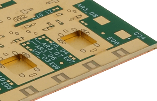
Furthermore, the choice of copper foil used in RF PCBs also plays a significant role in their performance.
High-frequency signals are particularly sensitive to surface roughness, which can cause signal loss and degradation. Therefore, smooth copper foils, such as rolled annealed (RA) copper, are often preferred over electro-deposited (ED) copper. RA copper provides a smoother surface, reducing signal attenuation and improving overall performance.
In conclusion, the materials used in RF PCB manufacturing are critical to the performance and reliability of the final product. PTFE, Rogers materials, ceramic-filled laminates, and liquid crystal polymers each offer unique properties that make them suitable for different high-frequency applications. Additionally, the choice of copper foil can significantly impact signal integrity. By carefully selecting the appropriate materials, manufacturers can ensure that their RF PCBs meet the stringent requirements of modern high-frequency electronic devices.
Challenges And Solutions In RF PCB Fabrication
Radio frequency printed circuit boards (RF PCBs) are integral to the functionality of modern communication systems, including wireless networks, satellite communications, and radar systems. However, the fabrication of RF PCBs presents a unique set of challenges that require specialized solutions to ensure optimal performance and reliability.
One of the primary challenges in RF PCB fabrication is the selection of suitable materials.
Unlike standard PCBs, RF PCBs operate at high frequencies, necessitating materials with low dielectric constants and low loss tangents to minimize signal attenuation and phase distortion. Materials such as PTFE (polytetrafluoroethylene) and ceramic-filled laminates are often preferred, but they come with their own set of processing difficulties, including higher costs and more complex handling requirements.
Another significant challenge is maintaining signal integrity.
At high frequencies, even minor imperfections in the PCB layout can lead to significant signal degradation. This necessitates meticulous attention to trace width, spacing, and the overall layout design. Impedance control becomes critical, requiring precise calculations and often necessitating the use of advanced simulation tools to predict and mitigate potential issues. Additionally, the presence of parasitic elements, such as unwanted capacitance and inductance, can further complicate the design process. To address these issues, designers often employ techniques such as differential signaling and the use of ground planes to provide a stable reference and reduce electromagnetic interference (EMI).
Thermal management is another crucial aspect that cannot be overlooked.
RF components tend to generate significant amounts of heat, which can adversely affect performance and longevity. Effective thermal management strategies, such as the use of thermal vias, heat sinks, and appropriate material selection, are essential to dissipate heat efficiently. Moreover, the integration of RF components with other electronic components on the same PCB can lead to additional thermal challenges, necessitating a holistic approach to thermal design.
Manufacturing tolerances also pose a considerable challenge in RF PCB fabrication.
The precision required for high-frequency applications means that even slight deviations in manufacturing processes can lead to performance issues. Advanced manufacturing techniques, such as laser direct imaging (LDI) and precision drilling, are often employed to achieve the necessary tolerances. Furthermore, stringent quality control measures, including automated optical inspection (AOI) and electrical testing, are essential to ensure that the fabricated PCBs meet the required specifications.
In addition to these technical challenges, the rapid pace of technological advancements in the RF domain necessitates continuous innovation and adaptation.
As frequencies continue to increase and applications become more demanding, the need for novel materials and fabrication techniques becomes ever more pressing. Collaborative efforts between material scientists, PCB designers, and manufacturers are crucial to developing solutions that can keep pace with these evolving requirements.
In conclusion, the fabrication of RF PCBs is a complex and multifaceted process that demands a deep understanding of material properties, signal integrity, thermal management, and manufacturing precision. While the challenges are significant, ongoing advancements in materials science, design methodologies, and manufacturing technologies offer promising solutions. By addressing these challenges through a combination of innovative techniques and rigorous quality control, it is possible to produce RF PCBs that meet the high-performance standards required for modern communication systems.