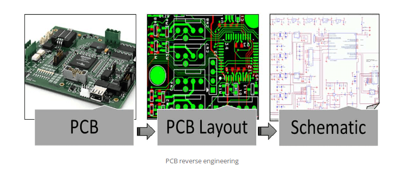
Reverse engineering multilayer pcb
Techniques For Reverse Engineering Multilayer PCBs
Reverse engineering multilayer printed circuit boards (PCBs) is a complex yet essential process in various fields, including electronics repair, product development, and competitive analysis.
This intricate task involves deconstructing a PCB to understand its design, functionality, and components. To achieve this, several techniques are employed, each contributing to a comprehensive understanding of the multilayer PCB’s architecture.
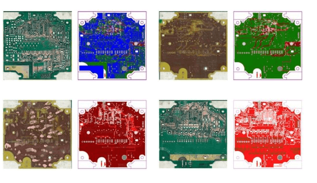
Initially, visual inspection serves as the first step in reverse engineering.
This technique involves examining the PCB with the naked eye or using magnification tools to identify visible components, traces, and solder joints. While this method provides a general overview, it is limited in its ability to reveal the internal layers and hidden connections of a multilayer PCB. Therefore, it is often supplemented with more advanced techniques.
One such advanced technique is X-ray imaging, which allows for non-destructive examination of the PCB’s internal structure.
By using X-rays, engineers can visualize the internal layers, vias, and buried components without physically damaging the board. This method is particularly useful for identifying the layout and interconnections of multilayer PCBs, providing a clear picture of the board’s internal complexity.
Following X-ray imaging, de-soldering and component removal are often necessary to gain a deeper understanding of the PCB’s design.
This process involves carefully removing components from the board to examine the underlying traces and connections. Specialized tools, such as hot air rework stations and soldering irons, are used to ensure that components are removed without causing damage to the PCB. Once the components are removed, the board can be scanned or photographed to create a detailed map of the traces and connections.
To further analyze the PCB, engineers may employ chemical etching techniques.
This method involves using chemical solutions to remove specific layers of the PCB, revealing the underlying traces and connections. By sequentially etching away each layer, engineers can reconstruct the entire multilayer structure of the PCB. This technique, while effective, requires careful handling of chemicals and precise control to avoid damaging the board.
In addition to physical examination methods, software tools play a crucial role in reverse engineering multilayer PCBs.
Computer-aided design (CAD) software can be used to create digital representations of the PCB based on the information gathered from visual inspection, X-ray imaging, and component removal. These digital models allow engineers to simulate the PCB’s functionality, analyze signal integrity, and identify potential design flaws. Furthermore, specialized reverse engineering software can assist in automating the process of trace extraction and component identification, significantly reducing the time and effort required.
Another important technique is the use of electrical testing and measurement.
By applying test signals and measuring the responses at various points on the PCB, engineers can infer the functionality and connectivity of different components and traces. This method is particularly useful for verifying the accuracy of the reconstructed digital model and ensuring that the reverse-engineered PCB functions as intended.
In conclusion, reverse engineering multilayer PCBs involves a combination of visual inspection, X-ray imaging, component removal, chemical etching, software tools, and electrical testing. Each technique contributes to a comprehensive understanding of the PCB’s design and functionality, enabling engineers to reconstruct and analyze complex multilayer boards. By employing these techniques, engineers can gain valuable insights into existing designs, facilitate repairs, and drive innovation in electronic product development.
Tools And Software For Multilayer PCB Reverse Engineering
Reverse engineering multilayer printed circuit boards (PCBs) is a complex process that requires a combination of specialized tools and software to accurately deconstruct and analyze the intricate layers and components. The first step in this process typically involves the use of high-resolution imaging tools. Scanning Electron Microscopes (SEMs) and X-ray imaging systems are indispensable for capturing detailed images of the PCB’s internal structure. These tools allow engineers to visualize the multiple layers without physically dismantling the board, thereby preserving its integrity for further analysis.
Once the imaging is complete, the next phase involves the use of software to interpret and reconstruct the data.
Computer-Aided Design (CAD) software, such as Altium Designer or Autodesk Eagle, is often employed to create a digital representation of the PCB. These programs offer advanced features that facilitate the mapping of electrical connections and the identification of components. By importing the high-resolution images into the CAD software, engineers can trace the pathways and connections, layer by layer, to build a comprehensive schematic of the board.
In addition to CAD software, specialized reverse engineering tools like Gerber file viewers and editors are crucial.
Gerber files are the standard format for PCB design data, and tools like Gerbv or ViewMate allow engineers to examine these files in detail. By comparing the Gerber files with the reconstructed schematic, discrepancies can be identified and corrected, ensuring an accurate reverse engineering process. Furthermore, these tools often include features for editing and modifying the design, which can be useful for making improvements or adaptations to the original PCB.
Another essential tool in the reverse engineering toolkit is the use of circuit simulation software.
Programs like SPICE (Simulation Program with Integrated Circuit Emphasis) enable engineers to simulate the electrical behavior of the reconstructed PCB. This step is vital for verifying that the reverse-engineered design functions as intended. By simulating various operating conditions and stress tests, potential issues can be identified and addressed before any physical prototypes are created.
Moreover, the use of database management systems cannot be overlooked.
These systems, such as SQL-based databases, are used to store and manage the vast amounts of data generated during the reverse engineering process. Efficient data management ensures that all information is easily accessible and can be cross-referenced as needed. This is particularly important when dealing with complex multilayer PCBs, where the volume of data can be overwhelming.
In addition to these tools and software, collaboration platforms play a significant role in the reverse engineering process.
Platforms like GitHub or Bitbucket allow multiple engineers to work on the same project simultaneously, sharing data and updates in real-time. This collaborative approach not only speeds up the process but also ensures that different perspectives and expertise are brought to bear on the project, leading to more robust and innovative solutions.
Finally, it is important to mention the role of documentation and reporting tools.
Comprehensive documentation is essential for capturing the insights and findings from the reverse engineering process. Tools like Microsoft Visio or LaTeX can be used to create detailed reports and diagrams that document every aspect of the PCB’s design and functionality. This documentation serves as a valuable reference for future projects and can also be used to demonstrate compliance with industry standards and regulations.
In conclusion, reverse engineering multilayer PCBs is a multifaceted process that relies on a combination of high-resolution imaging tools, advanced CAD software, specialized reverse engineering tools, circuit simulation programs, database management systems, collaboration platforms, and documentation tools. Each of these components plays a crucial role in ensuring that the reverse engineering process is accurate, efficient, and effective.
Challenges And Solutions In Reverse Engineering Multilayer PCBs
Reverse engineering multilayer printed circuit boards (PCBs) presents a unique set of challenges that require specialized knowledge and sophisticated techniques. Multilayer PCBs, which consist of multiple layers of conductive material separated by insulating layers, are integral to modern electronic devices due to their ability to support complex circuitry in a compact form. However, the complexity of these boards also makes reverse engineering a daunting task.
One of the primary challenges in reverse engineering multilayer PCBs is the difficulty in accessing and visualizing the internal layers.
Unlike single-layer or double-layer PCBs, where the traces and components are relatively easy to inspect, multilayer PCBs conceal much of their circuitry within the internal layers. This necessitates the use of advanced imaging techniques such as X-ray tomography, which can provide a detailed view of the internal structure without physically damaging the board. However, X-ray tomography is not without its limitations; it requires expensive equipment and specialized expertise to interpret the resulting images accurately.
In addition to imaging challenges, the complexity of the circuitry itself poses significant hurdles.
Multilayer PCBs often incorporate intricate designs with numerous vias, blind vias, and buried vias that connect different layers. These connections are crucial for the board’s functionality but complicate the reverse engineering process. To address this, engineers often employ a combination of software tools and manual inspection. Computer-aided design (CAD) software can be used to recreate the board’s layout by tracing the connections and components. However, this process is time-consuming and requires a high level of precision to ensure that the recreated design accurately reflects the original.
Another challenge is the identification and characterization of components.
Multilayer PCBs frequently use surface-mount technology (SMT), which involves placing components directly onto the surface of the board. These components are often tiny and densely packed, making them difficult to identify and analyze. Furthermore, manufacturers may use proprietary or custom components that lack readily available documentation. In such cases, engineers must rely on techniques such as decapsulation, where the component’s outer casing is removed to reveal its internal structure. This allows for a more detailed analysis but also risks damaging the component.
Thermal management is another critical aspect that must be considered during the reverse engineering process.
Multilayer PCBs are designed to dissipate heat efficiently, but replicating this thermal performance in a reverse-engineered design can be challenging. Engineers must carefully analyze the thermal properties of the original board and ensure that the recreated design can manage heat effectively to prevent overheating and ensure reliable operation.
Despite these challenges, several solutions have been developed to facilitate the reverse engineering of multilayer PCBs.
Advances in imaging technology, such as high-resolution X-ray systems and 3D scanning, have significantly improved the ability to visualize internal layers. Additionally, sophisticated CAD software has become more capable of handling complex designs, allowing for more accurate recreations of the original board. Collaboration and knowledge sharing within the engineering community also play a crucial role, as engineers can leverage collective expertise and experience to overcome obstacles.
In conclusion, reverse engineering multilayer PCBs is a complex and demanding process that requires a combination of advanced techniques, specialized knowledge, and meticulous attention to detail. While significant challenges exist, ongoing advancements in technology and collaborative efforts within the engineering community continue to provide effective solutions, enabling engineers to successfully reverse engineer these intricate and essential components of modern electronics.
Case Studies: Successful Reverse Engineering Of Multilayer PCBs
Reverse engineering multilayer printed circuit boards (PCBs) is a complex yet fascinating process that has seen numerous successful case studies, each contributing to the advancement of technology and innovation. One notable example involves a telecommunications company that needed to replicate a legacy PCB for which the original design files were lost. This case study highlights the meticulous steps and sophisticated techniques employed to achieve a successful reverse engineering outcome.
Initially, the team began by carefully disassembling the multilayer PCB, a task that required precision to avoid damaging the intricate layers.
Each layer was meticulously photographed and documented, ensuring that every trace, via, and component was accurately captured. This visual documentation served as the foundation for reconstructing the PCB’s design.
Following the disassembly, the team employed advanced imaging techniques such as X-ray and CT scanning.
These methods provided detailed insights into the internal structure of the PCB, revealing hidden layers and buried vias that were not visible through traditional means. The high-resolution images obtained from these scans were crucial in understanding the complex interconnections within the multilayer PCB.
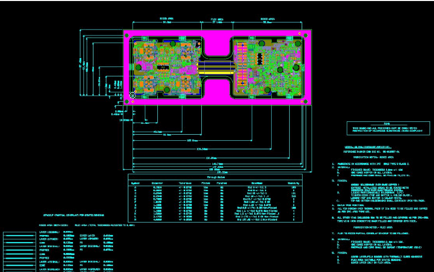
With the imaging data in hand, the next step involved creating a schematic diagram.
This process required a deep understanding of electronic circuits and components. Engineers meticulously traced each connection, ensuring that the reconstructed schematic accurately reflected the original design. This phase was particularly challenging due to the multilayer nature of the PCB, which often involved intricate routing and dense component placement.
Once the schematic was completed, the team moved on to the layout design.
Using specialized software, they recreated the PCB layout, layer by layer. This step demanded a high level of precision, as even minor deviations could result in functional discrepancies. The layout design was then cross-referenced with the original images and scans to ensure accuracy.
After finalizing the layout, the team proceeded to fabricate a prototype of the reverse-engineered PCB.
This involved selecting appropriate materials and manufacturing techniques to replicate the original board as closely as possible. The prototype underwent rigorous testing to verify its functionality and performance. Any discrepancies identified during testing were meticulously analyzed and corrected, ensuring that the final product met the required specifications.
Another compelling case study involves a medical device manufacturer that needed to reverse engineer a multilayer PCB used in a critical piece of diagnostic equipment.
The original manufacturer had gone out of business, leaving no design files or documentation. The reverse engineering team faced the daunting task of not only replicating the PCB but also ensuring that it met stringent medical standards.
In this case, the team employed a combination of non-destructive and destructive techniques.
Non-destructive methods, such as high-resolution optical microscopy and 3D laser scanning, provided detailed surface images. Destructive techniques, including layer-by-layer etching, were used to reveal the internal structure. This dual approach allowed the team to gather comprehensive data without compromising the integrity of the original PCB.
The reconstructed design underwent extensive validation, including electromagnetic compatibility (EMC) testing and thermal analysis. These tests ensured that the reverse-engineered PCB not only replicated the original design but also met the rigorous standards required for medical devices. The successful completion of this project not only restored the functionality of the diagnostic equipment but also provided the manufacturer with a reliable source for future production.
In conclusion, these case studies underscore the intricate and multifaceted nature of reverse engineering multilayer PCBs. Through a combination of advanced imaging techniques, meticulous documentation, and rigorous testing, engineers can successfully replicate complex PCBs, ensuring the continuity of critical technologies and devices.