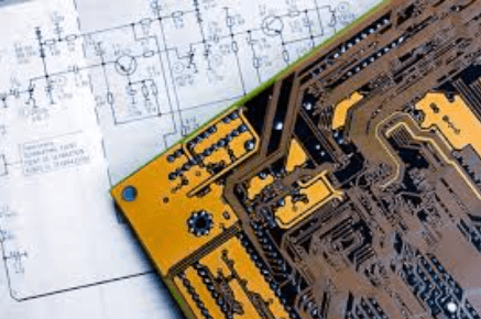
Rf pcb fabrication
Design Considerations For RF PCB Fabrication
Designing printed circuit boards (PCBs) for radio frequency (RF) applications requires meticulous attention to detail and a deep understanding of the unique challenges posed by high-frequency signals. Unlike standard PCBs, RF PCBs must manage signal integrity, minimize interference, and ensure efficient transmission of high-frequency signals. Therefore, several critical design considerations must be addressed to achieve optimal performance in RF PCB fabrication.
First and foremost, the choice of substrate material is paramount.
RF PCBs typically employ materials with low dielectric constants and low loss tangents to minimize signal loss and ensure stable signal propagation. Common materials include PTFE (Teflon), Rogers, and other specialized laminates designed for high-frequency applications. These materials, while more expensive than standard FR-4, provide the necessary electrical properties to support RF signal integrity.
Another crucial aspect is the layout and routing of the PCB.
Signal traces in RF PCBs must be carefully designed to maintain consistent impedance and minimize signal reflections. This often involves the use of controlled impedance traces, which require precise calculations and adherence to specific design rules. Microstrip and stripline configurations are commonly used to achieve controlled impedance, with microstrip traces being placed on the outer layers of the PCB and stripline traces sandwiched between layers. Additionally, the width and spacing of these traces must be meticulously controlled to maintain the desired impedance.
Ground planes play a vital role in RF PCB design, serving as a reference point for signal traces and helping to reduce electromagnetic interference (EMI).
A continuous ground plane beneath the signal traces can significantly improve signal integrity by providing a low-impedance return path for high-frequency currents. Furthermore, the use of via stitching, which involves placing multiple vias around the perimeter of the ground plane, can enhance the grounding and reduce the potential for EMI.
Component placement is another critical consideration in RF PCB design.
High-frequency components, such as amplifiers, mixers, and filters, should be strategically placed to minimize signal path lengths and reduce the potential for interference. Additionally, sensitive components should be shielded from noisy elements to prevent unwanted coupling. The use of shielding cans or enclosures can further mitigate EMI and improve overall performance.
Thermal management is also a key factor in RF PCB design.
High-frequency components can generate significant heat, which, if not properly managed, can degrade performance and reliability. Effective thermal management techniques, such as the use of thermal vias, heat sinks, and thermal pads, are essential to dissipate heat and maintain optimal operating temperatures.
Moreover, the choice of connectors and interconnects is critical in RF PCB design.
Coaxial connectors, such as SMA or SMB, are commonly used for their excellent high-frequency performance and low insertion loss. The placement and orientation of these connectors should be carefully considered to minimize signal degradation and ensure reliable connections.
In addition to these technical considerations, it is essential to collaborate closely with PCB manufacturers during the design process.
Manufacturers can provide valuable insights into material selection, fabrication capabilities, and design for manufacturability (DFM) guidelines. Early engagement with manufacturers can help identify potential issues and ensure that the design is optimized for production.
In conclusion, designing RF PCBs requires a comprehensive understanding of high-frequency signal behavior and meticulous attention to detail. By carefully selecting substrate materials, optimizing layout and routing, ensuring effective grounding, strategically placing components, managing thermal performance, and choosing appropriate connectors, designers can achieve high-performance RF PCBs that meet the stringent demands of modern RF applications. Close collaboration with PCB manufacturers further enhances the likelihood of success, resulting in reliable and efficient RF circuits.
Material Selection For High-Frequency RF PCBs
When it comes to the fabrication of high-frequency RF PCBs, material selection is a critical factor that significantly influences the performance, reliability, and overall functionality of the final product. The choice of materials must be meticulously considered to ensure that the PCB can handle the specific demands of high-frequency applications, which often involve complex signal integrity requirements and stringent performance criteria.
One of the primary considerations in material selection for high-frequency RF PCBs is the dielectric constant (Dk) of the substrate material.
The dielectric constant affects the speed at which signals propagate through the PCB, and variations in Dk can lead to signal distortion and loss. Therefore, materials with a stable and low dielectric constant are preferred for high-frequency applications. Common materials that meet these criteria include PTFE (Polytetrafluoroethylene), also known as Teflon, and ceramic-filled laminates. These materials offer excellent electrical properties, including low dielectric loss, which is essential for maintaining signal integrity at high frequencies.
In addition to the dielectric constant, the dissipation factor (Df) of the substrate material is another crucial parameter.
The dissipation factor measures the energy loss as the signal propagates through the material. A low dissipation factor is desirable because it minimizes signal attenuation and ensures that the signal strength remains consistent over long distances. Materials such as Rogers RO3000 and RO4000 series, which have low dissipation factors, are often used in high-frequency RF PCB applications due to their superior performance in minimizing signal loss.
Thermal management is another important aspect to consider when selecting materials for high-frequency RF PCBs.
High-frequency signals can generate significant amounts of heat, which can affect the performance and longevity of the PCB. Therefore, materials with good thermal conductivity are essential to dissipate heat effectively and maintain the stability of the PCB. Copper-clad laminates with high thermal conductivity are commonly used to enhance heat dissipation and ensure reliable operation under high-frequency conditions.
Moreover, the mechanical properties of the substrate material should not be overlooked.
High-frequency RF PCBs often require precise and intricate designs, which necessitate materials with good dimensional stability and mechanical strength. Materials such as FR-4, although widely used in general PCB applications, may not always be suitable for high-frequency RF PCBs due to their relatively higher dielectric constant and dissipation factor. Instead, materials like PTFE and ceramic-filled laminates, which offer better mechanical properties and stability, are preferred.
Furthermore, the compatibility of the substrate material with the manufacturing processes is a vital consideration. High-frequency RF PCBs often involve advanced fabrication techniques such as laser drilling, precision etching, and fine-line circuitry. Therefore, the selected material must be compatible with these processes to ensure high-quality and reliable PCB production. Materials that can withstand the rigors of advanced manufacturing processes without compromising their electrical and mechanical properties are ideal for high-frequency RF PCB fabrication.
In conclusion, the selection of materials for high-frequency RF PCBs is a multifaceted process that requires careful consideration of various factors, including the dielectric constant, dissipation factor, thermal management, mechanical properties, and manufacturing compatibility. By choosing the appropriate materials, designers can ensure that the high-frequency RF PCBs meet the stringent performance requirements and deliver reliable and efficient operation in demanding applications.
Challenges In RF PCB Manufacturing And How To Overcome Them
RF PCB fabrication presents a unique set of challenges that distinguish it from standard PCB manufacturing. These challenges stem from the high-frequency signals that RF circuits handle, which necessitate meticulous attention to detail in design, material selection, and manufacturing processes. Understanding these challenges and implementing strategies to overcome them is crucial for producing reliable and high-performance RF PCBs.
One of the primary challenges in RF PCB manufacturing is signal integrity.
High-frequency signals are susceptible to various forms of interference and loss, which can degrade performance. To mitigate these issues, careful consideration must be given to the layout and routing of the PCB. For instance, maintaining consistent impedance throughout the signal paths is essential. This can be achieved by using controlled impedance traces and ensuring that the PCB stack-up is designed to support the required impedance levels. Additionally, minimizing the length of signal paths and avoiding sharp bends can help reduce signal degradation.
Another significant challenge is the selection of materials.
The dielectric properties of the substrate material play a crucial role in the performance of RF circuits. Materials with low dielectric constant (Dk) and low loss tangent (Df) are preferred for RF applications because they minimize signal loss and ensure better signal propagation. However, these materials can be more expensive and difficult to work with compared to standard FR-4 substrates. Manufacturers must balance performance requirements with cost considerations, often opting for specialized materials like Rogers or Teflon-based laminates for high-frequency applications.
Thermal management is also a critical concern in RF PCB fabrication.
High-frequency circuits can generate significant amounts of heat, which can affect the performance and reliability of the PCB. Effective thermal management strategies, such as the use of thermal vias, heat sinks, and proper placement of heat-generating components, are essential to dissipate heat efficiently. Additionally, selecting materials with good thermal conductivity can help manage heat more effectively.
Manufacturing tolerances present another challenge in RF PCB fabrication.
The precision required for high-frequency circuits is much greater than that for standard PCBs. Even slight variations in trace width, spacing, or layer thickness can significantly impact the performance of the RF circuit. To address this, manufacturers must employ advanced fabrication techniques and maintain stringent quality control measures. This includes using high-precision equipment for drilling, etching, and plating processes, as well as implementing thorough inspection and testing protocols to ensure that the final product meets the required specifications.
Electromagnetic interference (EMI) is a further complication in RF PCB design.
High-frequency signals can easily radiate and couple with other signals, leading to unwanted interference. To mitigate EMI, designers can use techniques such as proper grounding, shielding, and the use of guard traces. Additionally, careful placement of components and the use of differential signaling can help reduce the susceptibility to EMI.
In conclusion, RF PCB fabrication involves a complex interplay of factors that must be carefully managed to ensure optimal performance. By addressing challenges related to signal integrity, material selection, thermal management, manufacturing tolerances, and EMI, manufacturers can produce high-quality RF PCBs that meet the demanding requirements of modern high-frequency applications. Through meticulous design, advanced fabrication techniques, and rigorous quality control, the obstacles inherent in RF PCB manufacturing can be effectively overcome, paving the way for reliable and efficient RF circuits.
Advanced Techniques In RF PCB Prototyping
In the realm of modern electronics, Radio Frequency (RF) Printed Circuit Boards (PCBs) play a pivotal role in the functionality of various high-frequency applications, including telecommunications, radar systems, and wireless networks. The fabrication of RF PCBs demands a meticulous approach, given the sensitivity and precision required to handle high-frequency signals. Advanced techniques in RF PCB prototyping have emerged to address these challenges, ensuring optimal performance and reliability.
One of the foremost considerations in RF PCB fabrication is the selection of appropriate materials.
Unlike standard PCBs, RF PCBs require substrates with low dielectric constants and minimal loss tangents to maintain signal integrity. Materials such as Rogers, Taconic, and PTFE (Polytetrafluoroethylene) are commonly used due to their superior electrical properties. These materials help in minimizing signal loss and ensuring consistent impedance, which is crucial for high-frequency applications.
Transitioning from material selection to design considerations, the layout of an RF PCB is another critical aspect.
The design must account for factors such as trace width, spacing, and the overall geometry of the circuit. Microstrip and stripline configurations are often employed to control impedance and reduce signal reflections. Additionally, the use of ground planes and proper grounding techniques is essential to mitigate electromagnetic interference (EMI) and crosstalk between adjacent traces. Advanced simulation tools, such as electromagnetic field solvers, are utilized to model and optimize the RF PCB design before actual fabrication.
Moving forward, the fabrication process itself involves several advanced techniques to ensure precision and accuracy.
Laser direct imaging (LDI) is one such technique that has gained prominence. LDI allows for the creation of fine features and intricate patterns with high resolution, which is particularly beneficial for RF circuits that require tight tolerances. Furthermore, the use of controlled-depth drilling and laser drilling techniques enables the creation of microvias and blind vias, which are essential for multi-layer RF PCBs. These vias facilitate interconnections between different layers without compromising signal integrity.
Another critical aspect of RF PCB prototyping is the surface finish.
The choice of surface finish can significantly impact the performance of high-frequency signals. Electroless nickel immersion gold (ENIG) and immersion silver are popular choices due to their excellent conductivity and corrosion resistance. These finishes provide a smooth and uniform surface, which is vital for maintaining consistent impedance and reducing signal loss.
In addition to the aforementioned techniques, the testing and validation of RF PCBs are paramount to ensure their functionality. Vector network analyzers (VNAs) and time-domain reflectometers (TDRs) are commonly used to measure parameters such as return loss, insertion loss, and impedance. These measurements help in identifying any discrepancies or defects in the PCB, allowing for necessary adjustments and refinements.
As we delve deeper into the advancements in RF PCB prototyping, it becomes evident that a holistic approach encompassing material selection, design optimization, precise fabrication techniques, and rigorous testing is essential. The integration of these advanced techniques not only enhances the performance and reliability of RF PCBs but also paves the way for innovation in high-frequency applications. Consequently, staying abreast of these advancements is crucial for engineers and designers striving to push the boundaries of what is possible in the ever-evolving field of RF technology.