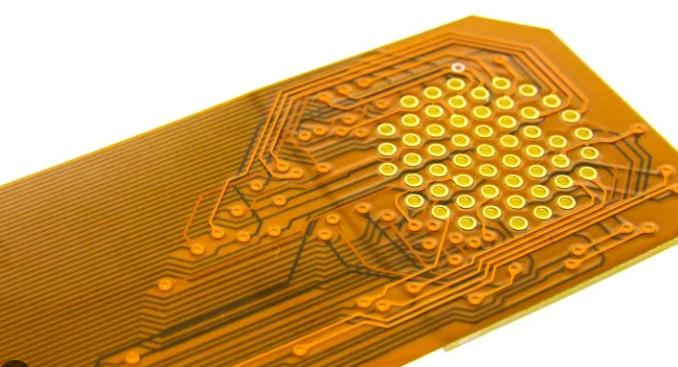
Flex pcb through hole
Advantages Of Flex PCB Through Hole Technology
Flex PCB through hole technology offers a multitude of advantages that make it an attractive option for various electronic applications.
One of the primary benefits is its ability to provide enhanced mechanical stability.
Through hole components are inserted into pre-drilled holes on the flexible printed circuit board and soldered on the opposite side, creating a robust mechanical bond. This ensures that the components remain securely attached, even under conditions of mechanical stress or vibration, which is particularly advantageous in applications such as automotive and aerospace industries where reliability is paramount.
In addition to mechanical stability, flex PCB through hole technology also offers superior electrical connectivity.
The through hole method allows for a more reliable electrical connection between the component leads and the circuit board. This is because the solder joint surrounds the entire lead, providing a larger contact area compared to surface mount technology (SMT). Consequently, this results in lower resistance and better current-carrying capacity, which is crucial for high-power applications.
Another significant advantage of flex PCB through hole technology is its compatibility with a wide range of components.
While SMT is limited to components that can be mounted on the surface of the board, through hole technology can accommodate both axial and radial leaded components. This versatility allows for greater design flexibility, enabling engineers to incorporate a diverse array of components into their designs. Furthermore, through hole components are generally easier to handle and place manually, which can be beneficial during the prototyping phase or for low-volume production runs.
Moreover, flex PCB through hole technology enhances thermal management capabilities.
The through holes can act as thermal vias, allowing heat to dissipate more effectively from the components to the surrounding environment. This is particularly important in high-power applications where efficient heat dissipation is critical to maintaining the performance and longevity of the electronic device. By facilitating better thermal management, through hole technology helps prevent overheating and potential damage to the components and the circuit board.
Additionally, flex PCB through hole technology offers improved durability and longevity.
The robust mechanical and electrical connections provided by through hole components contribute to the overall durability of the electronic device. This is especially beneficial in harsh environments where the device may be subjected to extreme temperatures, humidity, or mechanical shocks. The enhanced durability ensures that the device can withstand these challenging conditions without compromising its performance.
Furthermore, the use of flex PCB through hole technology can lead to cost savings in certain applications.
While the initial manufacturing process may be more complex and time-consuming compared to SMT, the long-term benefits of increased reliability, durability, and performance can outweigh the initial costs. This is particularly true for applications where the cost of device failure is high, such as in medical devices or critical communication systems.
In conclusion, flex PCB through hole technology offers numerous advantages that make it a valuable option for various electronic applications. Its ability to provide enhanced mechanical stability, superior electrical connectivity, compatibility with a wide range of components, improved thermal management, and increased durability make it an attractive choice for engineers and designers. By leveraging these benefits, flex PCB through hole technology can contribute to the development of reliable, high-performance electronic devices that can withstand the demands of challenging environments.
Design Considerations For Flex PCB Through Hole Applications
When designing flex PCB through hole applications, several critical considerations must be taken into account to ensure optimal performance and reliability. Flex PCBs, or flexible printed circuit boards, offer unique advantages such as reduced weight, space savings, and the ability to conform to complex geometries. However, the integration of through holes in these flexible substrates introduces additional complexities that must be meticulously addressed during the design phase.
One of the primary considerations is the material selection for the flex PCB.
The substrate material must possess excellent flexibility and durability to withstand repeated bending and flexing without compromising the integrity of the through holes. Polyimide is a commonly used material due to its superior thermal stability and mechanical properties. Additionally, the copper used for the conductive traces must be carefully chosen to ensure it can endure the mechanical stresses imposed by the flexing action.
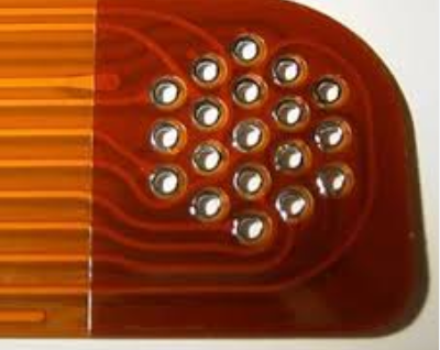
The layout of the through holes is another crucial aspect.
Proper spacing and alignment are essential to prevent mechanical stress concentrations that could lead to cracking or delamination. Designers must also consider the aspect ratio of the through holes, which is the ratio of the hole depth to its diameter. A higher aspect ratio can pose challenges during the manufacturing process, such as difficulties in plating the hole walls uniformly. Therefore, maintaining an optimal aspect ratio is vital for ensuring reliable electrical connections.
Furthermore, the placement of through holes should be strategically planned to avoid areas of high mechanical stress.
For instance, placing through holes near bend lines or in regions that experience frequent flexing can significantly reduce the lifespan of the flex PCB. Instead, through holes should be located in areas that experience minimal mechanical strain. This strategic placement helps in maintaining the structural integrity of the flex PCB and ensures long-term reliability.
Thermal management is another important consideration in the design of flex PCB through hole applications.
The thermal expansion properties of the materials used must be compatible to prevent issues such as warping or delamination. Additionally, adequate thermal vias and heat dissipation mechanisms should be incorporated to manage the heat generated by the electronic components. Effective thermal management not only enhances the performance of the flex PCB but also extends its operational lifespan.
The manufacturing process for flex PCBs with through holes also demands careful attention.
Techniques such as laser drilling or mechanical drilling can be employed to create the through holes, each with its own set of advantages and limitations. Laser drilling offers high precision and is suitable for creating small-diameter holes, while mechanical drilling is more cost-effective for larger holes. The choice of drilling technique should align with the specific requirements of the application to achieve the desired balance between precision and cost.
In addition to these technical considerations, designers must also adhere to industry standards and guidelines to ensure the flex PCB meets the required quality and reliability benchmarks. Standards such as IPC-2223 provide comprehensive guidelines for the design and fabrication of flex PCBs, including recommendations for through hole design. Adhering to these standards helps in achieving consistent quality and facilitates easier integration with other electronic components.
In conclusion, the design of flex PCB through hole applications involves a multifaceted approach that encompasses material selection, layout planning, thermal management, and adherence to industry standards. By meticulously addressing these considerations, designers can create robust and reliable flex PCBs that leverage the unique advantages of flexible substrates while ensuring the integrity and performance of through hole connections.
Common Challenges In Flex PCB Through Hole Manufacturing
Flex PCB through hole manufacturing presents a unique set of challenges that can complicate the production process and impact the final product’s performance. One of the primary difficulties lies in the inherent flexibility of the substrate material. Unlike rigid PCBs, flex PCBs are made from materials such as polyimide or polyester, which can bend and twist. This flexibility, while advantageous for certain applications, introduces complications during the drilling and plating processes. Ensuring that the holes are accurately drilled and properly plated without damaging the substrate requires precise control and specialized equipment.
Another significant challenge is maintaining the integrity of the through holes during the thermal cycling that occurs in the manufacturing process.
Flex PCBs often undergo multiple heating and cooling cycles, which can cause expansion and contraction of the materials. This thermal stress can lead to issues such as delamination or cracking around the through holes, compromising the electrical connectivity and mechanical stability of the PCB. To mitigate these risks, manufacturers must carefully select materials with compatible thermal expansion coefficients and employ advanced techniques to reinforce the through holes.
The plating process itself also poses challenges.
Achieving a uniform and reliable copper plating inside the through holes is critical for ensuring good electrical conductivity. However, the flexible nature of the substrate can make it difficult to achieve consistent plating thickness. Variations in plating can lead to weak spots that are prone to failure under mechanical stress or during thermal cycling. To address this, manufacturers often use specialized plating baths and agitation techniques to ensure even distribution of the plating material.
Moreover, the design of flex PCBs can complicate the through hole manufacturing process.
Flex PCBs are often designed with complex geometries and tight tolerances to fit into compact and irregularly shaped spaces. This complexity can make it challenging to align the drilling and plating processes accurately. Any misalignment can result in off-center holes or incomplete plating, which can affect the performance and reliability of the final product. Advanced computer-aided design (CAD) tools and precision manufacturing equipment are essential to overcome these design-related challenges.
Additionally, the inspection and testing of flex PCBs with through holes present their own set of difficulties.
Traditional inspection methods, such as visual inspection or X-ray imaging, may not be sufficient to detect all potential defects in the through holes. Advanced inspection techniques, such as automated optical inspection (AOI) and electrical testing, are often required to ensure the quality and reliability of the through holes. These methods can be more time-consuming and costly, but they are essential for identifying and addressing defects before the PCBs are assembled into final products.
Furthermore, the environmental conditions during the manufacturing process can also impact the quality of the through holes.
Factors such as humidity, temperature, and cleanliness of the manufacturing environment can affect the adhesion of the plating material and the overall integrity of the through holes. Maintaining strict environmental controls and implementing cleanroom practices can help mitigate these risks and ensure consistent quality.
In conclusion, flex PCB through hole manufacturing involves a range of challenges that require careful consideration and advanced techniques to overcome. From the flexibility of the substrate material to the complexities of the plating process and the need for precise alignment and inspection, each step presents potential obstacles that can impact the final product’s performance and reliability. By understanding and addressing these challenges, manufacturers can produce high-quality flex PCBs that meet the demanding requirements of modern electronic applications.
Innovations In Flex PCB Through Hole Assembly Techniques
Flex PCB through hole assembly techniques have undergone significant innovations in recent years, driven by the increasing demand for more compact, reliable, and versatile electronic devices. These advancements are crucial as they address the unique challenges posed by flexible printed circuit boards (PCBs), which are widely used in various applications, from consumer electronics to medical devices and aerospace technology. The evolution of these techniques not only enhances the performance and durability of flex PCBs but also expands their potential applications.
One of the primary innovations in flex PCB through hole assembly is the development of advanced drilling technologies.
Traditional mechanical drilling methods often struggle with the delicate and flexible nature of these PCBs, leading to potential damage and reduced reliability. However, the advent of laser drilling has revolutionized this process. Laser drilling offers precision and control, allowing for the creation of clean, accurate holes without compromising the integrity of the flexible substrate. This method significantly reduces the risk of defects and enhances the overall quality of the through hole connections.
In addition to drilling advancements, the materials used in flex PCB through hole assembly have also seen substantial improvements.
The introduction of high-performance, flexible dielectric materials has been a game-changer. These materials provide excellent thermal stability, mechanical strength, and electrical insulation, which are essential for maintaining the integrity of through hole connections under various operating conditions. Moreover, the use of advanced adhesives and bonding techniques ensures that the components remain securely attached to the flexible substrate, even in demanding environments.
Another noteworthy innovation is the implementation of automated assembly processes.
Automation has brought a new level of precision and efficiency to flex PCB through hole assembly. Automated pick-and-place machines, equipped with advanced vision systems, can accurately position and insert components into the through holes, minimizing human error and increasing production speed. This not only improves the consistency and reliability of the assemblies but also reduces manufacturing costs, making flex PCBs more accessible for a wider range of applications.
Furthermore, the integration of advanced inspection and testing methods has played a crucial role in enhancing the reliability of flex PCB through hole assemblies.
Techniques such as automated optical inspection (AOI) and X-ray inspection allow for the thorough examination of through hole connections, identifying potential defects that may not be visible to the naked eye. These inspection methods ensure that only high-quality assemblies proceed to the next stages of production, thereby reducing the likelihood of failures in the final product.
The continuous miniaturization of electronic components has also driven innovations in flex PCB through hole assembly techniques.
As devices become smaller and more complex, the need for precise and reliable through hole connections becomes even more critical. Innovations such as micro-via technology, which involves the creation of extremely small through holes, have enabled the development of highly compact and densely populated flex PCBs. This technology allows for greater design flexibility and the integration of more functionality into smaller form factors.
In conclusion, the innovations in flex PCB through hole assembly techniques have significantly advanced the capabilities and applications of flexible printed circuit boards. From laser drilling and high-performance materials to automated assembly processes and advanced inspection methods, these advancements have addressed the unique challenges of working with flexible substrates. As a result, flex PCBs are now more reliable, efficient, and versatile, paving the way for their use in an ever-expanding array of electronic devices and systems.