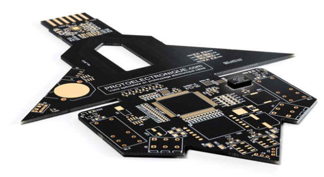
Pcb assembly rapid prototyping
Benefits Of Rapid Prototyping In PCB Assembly
Rapid prototyping in PCB assembly has revolutionized the electronics industry, offering a multitude of benefits that streamline the development process and enhance the overall quality of electronic products.
One of the primary advantages of rapid prototyping is the significant reduction in development time.
Traditional PCB assembly methods often involve lengthy design and testing phases, which can delay product launches. Rapid prototyping, however, allows for the quick creation of functional prototypes, enabling engineers to test and refine their designs in a fraction of the time. This accelerated timeline not only speeds up the development cycle but also provides a competitive edge in the fast-paced electronics market.
In addition to time savings, rapid prototyping in PCB assembly also offers cost efficiency.
By identifying and addressing design flaws early in the development process, companies can avoid the high costs associated with reworking or scrapping faulty PCBs. The ability to produce multiple iterations of a prototype quickly and affordably allows for thorough testing and validation, ensuring that the final product meets all specifications and performance requirements. This iterative approach minimizes the risk of costly errors and enhances the overall reliability of the end product.
Moreover, rapid prototyping facilitates better communication and collaboration among design teams.
With the ability to produce tangible prototypes quickly, engineers, designers, and stakeholders can more effectively visualize and evaluate the design. This hands-on approach fosters a collaborative environment where feedback can be promptly incorporated, leading to more informed decision-making and a more cohesive development process. The tangible nature of prototypes also aids in demonstrating concepts to clients and investors, providing a clear representation of the product’s potential and functionality.
Another notable benefit of rapid prototyping in PCB assembly is the enhancement of product innovation.
The flexibility and speed of rapid prototyping encourage experimentation and creativity, allowing engineers to explore new ideas and design concepts without the constraints of traditional manufacturing processes. This freedom to innovate can lead to the development of cutting-edge technologies and unique solutions that set a product apart in the market. Additionally, the ability to quickly iterate and test different designs enables engineers to optimize the performance and functionality of the PCB, resulting in a superior final product.
Furthermore, rapid prototyping supports the customization and personalization of electronic products.
In an era where consumer preferences are increasingly diverse, the ability to tailor products to specific needs and requirements is a significant advantage. Rapid prototyping allows for the efficient production of customized PCBs, enabling companies to cater to niche markets and offer personalized solutions. This adaptability not only enhances customer satisfaction but also opens up new business opportunities and revenue streams.
Lastly, rapid prototyping in PCB assembly contributes to sustainability and environmental responsibility.
By reducing the need for multiple production runs and minimizing material waste, rapid prototyping promotes more efficient use of resources. The ability to quickly identify and rectify design issues also reduces the likelihood of producing defective products, further minimizing waste and environmental impact. As sustainability becomes an increasingly important consideration in the electronics industry, the eco-friendly aspects of rapid prototyping are a valuable benefit.
In conclusion, the benefits of rapid prototyping in PCB assembly are manifold, encompassing time and cost efficiency, enhanced collaboration, increased innovation, customization capabilities, and environmental sustainability. As the electronics industry continues to evolve, the adoption of rapid prototyping techniques will undoubtedly play a crucial role in driving progress and maintaining a competitive edge.
Key Steps In PCB Assembly Rapid Prototyping
PCB assembly rapid prototyping is a critical process in the development of electronic devices, enabling engineers to quickly test and refine their designs before moving to mass production. This process involves several key steps, each of which plays a vital role in ensuring the functionality and reliability of the final product. Understanding these steps can help streamline the prototyping phase and reduce the time and cost associated with bringing a new electronic product to market.
The first step in PCB assembly rapid prototyping is the design phase.
During this phase, engineers create a detailed schematic of the circuit, specifying the components and their connections. This schematic serves as a blueprint for the PCB layout, which is the next step in the process. The layout involves arranging the components on the board and routing the electrical connections between them. Advanced software tools are often used to assist with this task, ensuring that the layout is optimized for performance and manufacturability.
Once the design and layout are finalized, the next step is to fabricate the PCB.
This involves creating a physical board based on the layout, typically using a combination of photolithography and etching techniques. The board is then drilled to create holes for through-hole components and vias, which are used to connect different layers of the PCB. After fabrication, the board undergoes a series of inspections to ensure that it meets the required specifications and is free of defects.
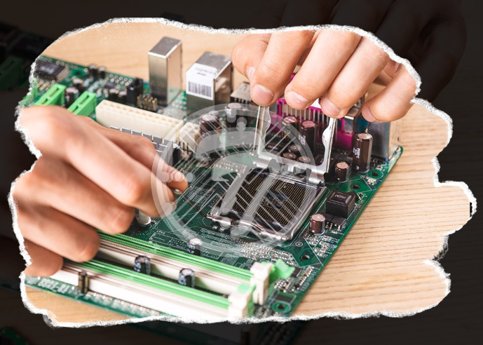
Following fabrication, the next step is to assemble the PCB.
This involves placing the components on the board and soldering them in place. There are two main types of components used in PCB assembly: surface-mount devices (SMDs) and through-hole components. SMDs are placed on the surface of the board and soldered using a reflow oven, while through-hole components are inserted into the drilled holes and soldered using a wave soldering machine. The choice of assembly method depends on the specific requirements of the design and the types of components used.
After assembly, the PCB undergoes a series of tests to verify its functionality.
These tests can include electrical testing, where the board is checked for continuity and proper operation of the circuit, as well as functional testing, where the board is tested in the context of its intended application. Any issues identified during testing are addressed through a process of debugging and rework, which may involve replacing faulty components or making adjustments to the layout.
Once the PCB has passed all tests, it is ready for integration into the final product.
This may involve additional steps such as programming microcontrollers, installing firmware, and performing system-level tests to ensure that the product operates as intended. Throughout this process, it is important to maintain thorough documentation, including design files, test results, and any changes made during debugging and rework. This documentation is essential for ensuring traceability and facilitating future iterations of the design.
In conclusion, PCB assembly rapid prototyping is a complex and multi-faceted process that requires careful planning and execution. By following these key steps—design, layout, fabrication, assembly, testing, and integration—engineers can efficiently develop and refine their electronic products, ultimately reducing time to market and improving product quality. The use of advanced tools and techniques, combined with rigorous testing and documentation, ensures that each prototype meets the necessary standards and performs reliably in its intended application.
Choosing The Right Materials For PCB Prototyping
When embarking on the journey of PCB assembly rapid prototyping, selecting the appropriate materials is a critical step that can significantly influence the performance, reliability, and manufacturability of the final product. The choice of materials not only affects the electrical properties of the PCB but also its mechanical strength, thermal stability, and overall cost. Therefore, understanding the various material options and their respective advantages and limitations is essential for making informed decisions.
To begin with, the substrate material forms the foundation of any PCB and is typically made from a dielectric material that provides insulation between the conductive layers.
The most commonly used substrate material is FR-4, a composite made from woven fiberglass cloth with an epoxy resin binder. FR-4 is favored for its excellent balance of mechanical strength, electrical insulation, and cost-effectiveness. However, for applications requiring higher performance, such as high-frequency circuits or environments with extreme temperatures, alternative materials like polyimide, PTFE (Teflon), or ceramic substrates may be more suitable. These materials offer superior thermal stability and lower dielectric losses, albeit at a higher cost.
In addition to the substrate, the choice of copper cladding is another crucial consideration.
Copper is the standard material for conductive traces due to its excellent electrical conductivity and ease of etching. The thickness of the copper layer, typically measured in ounces per square foot, can vary depending on the current-carrying requirements of the circuit. Standard copper thicknesses are 1 oz/ft², but for high-power applications, thicker copper layers such as 2 oz/ft² or even 3 oz/ft² may be necessary to handle higher currents without excessive heating.
Furthermore, the solder mask, which is a protective layer applied over the copper traces, plays a vital role in preventing short circuits and protecting the PCB from environmental factors such as moisture and dust.
The most common solder mask material is epoxy liquid photoimageable (LPI) solder mask, which offers good adhesion, chemical resistance, and ease of application. However, for high-frequency applications, a solder mask with lower dielectric constant and loss tangent, such as a liquid crystal polymer (LCP) solder mask, may be preferred to minimize signal degradation.
Another important material consideration is the type of surface finish applied to the exposed copper pads, which ensures good solderability and protects against oxidation.
Common surface finishes include HASL (Hot Air Solder Leveling), ENIG (Electroless Nickel Immersion Gold), and OSP (Organic Solderability Preservative). HASL is cost-effective and provides a robust solder joint, but its uneven surface can be problematic for fine-pitch components. ENIG, on the other hand, offers a flat and smooth surface, making it ideal for high-density interconnects and fine-pitch components, though it is more expensive. OSP is an environmentally friendly option that provides good solderability but may not be suitable for long-term storage.
Lastly, the selection of components and their compatibility with the chosen PCB materials must be carefully considered. Components with different thermal expansion coefficients can lead to mechanical stress and potential failure during thermal cycling. Therefore, matching the thermal properties of the PCB materials with those of the components is crucial for ensuring long-term reliability.
In conclusion, choosing the right materials for PCB prototyping involves a careful balance of electrical performance, mechanical strength, thermal stability, and cost. By thoroughly understanding the properties and trade-offs of various materials, designers can make informed decisions that optimize the performance and reliability of their PCB assemblies. This meticulous selection process is fundamental to the success of rapid prototyping and ultimately, the development of high-quality electronic products.
Common Challenges In PCB Assembly Rapid Prototyping
PCB assembly rapid prototyping is a critical phase in the development of electronic devices, allowing engineers to test and refine their designs before mass production. However, this process is not without its challenges.
One of the most significant issues faced during PCB assembly rapid prototyping is the complexity of design.
As electronic devices become more sophisticated, the designs of PCBs have become increasingly intricate. This complexity can lead to difficulties in ensuring that all components are correctly placed and connected, which is essential for the functionality of the final product.
Another common challenge is the availability of components.
In the rapid prototyping phase, engineers often require specific components that may not be readily available. This can lead to delays in the prototyping process, as sourcing these components can take time. Additionally, the use of substitute components can result in variations in performance, which can complicate the testing and refinement process.
Transitioning from design to physical assembly also presents its own set of challenges.
The precision required in placing and soldering components onto the PCB is paramount. Any misalignment or poor soldering can lead to short circuits or open circuits, which can render the prototype non-functional. This necessitates a high level of skill and attention to detail from the technicians involved in the assembly process.
Furthermore, the testing phase of PCB assembly rapid prototyping can be fraught with difficulties.
Identifying and diagnosing issues in a complex PCB can be time-consuming and requires specialized equipment and expertise. Engineers must meticulously test each aspect of the PCB to ensure that it meets the required specifications and performs as expected. This process can be iterative, with multiple rounds of testing and modification needed to achieve the desired outcome.
Cost is another significant factor in PCB assembly rapid prototyping.
The need for specialized components, equipment, and skilled labor can make this phase of development quite expensive. Balancing the need for rapid iteration with budget constraints is a common challenge faced by many development teams. This often requires careful planning and resource management to ensure that the prototyping process remains within budget while still achieving the necessary results.
Moreover, communication and collaboration among team members are crucial during the rapid prototyping phase.
Miscommunication or lack of coordination can lead to errors in the design and assembly process, resulting in delays and increased costs. Effective project management and clear communication channels are essential to ensure that all team members are aligned and working towards the same goals.
In addition to these challenges, the rapid pace of technological advancement means that engineers must constantly stay updated with the latest tools, techniques, and components available for PCB assembly. This continuous learning curve can be demanding but is necessary to remain competitive and produce high-quality prototypes.
In conclusion, while PCB assembly rapid prototyping is an invaluable part of the electronic device development process, it is accompanied by a range of challenges. From the complexity of design and component availability to the precision required in assembly and the costs involved, each aspect requires careful consideration and management. By addressing these challenges effectively, development teams can ensure that their prototypes are functional, reliable, and ready for the next stage of production.
Innovations In PCB Assembly Rapid Prototyping Technology
The field of printed circuit board (PCB) assembly has witnessed significant advancements in recent years, particularly in the realm of rapid prototyping technology. These innovations have revolutionized the way electronic devices are designed, tested, and brought to market, offering unprecedented speed and efficiency. As the demand for more complex and compact electronic devices continues to grow, the need for advanced PCB assembly rapid prototyping technologies becomes increasingly critical.
One of the most notable innovations in PCB assembly rapid prototyping is the development of automated assembly machines.
3 These machines have drastically reduced the time required to assemble PCBs by automating the placement of components and soldering processes. Traditional methods, which relied heavily on manual labor, were not only time-consuming but also prone to human error. Automated assembly machines, on the other hand, ensure precision and consistency, significantly enhancing the overall quality of the final product. Moreover, these machines can handle a wide range of component sizes and types, making them versatile tools for various applications.
In addition to automated assembly machines, advancements in 3D printing technology have also played a crucial role in the evolution of PCB assembly rapid prototyping.
3D printing allows for the creation of complex PCB designs with intricate geometries that would be challenging to achieve using conventional manufacturing methods. This technology enables designers to quickly produce prototypes and test their functionality, thereby accelerating the development process. Furthermore, 3D printing reduces material waste and lowers production costs, making it an economically viable option for both small-scale and large-scale projects.
Another significant innovation in this field is the use of advanced software tools for PCB design and simulation.
Modern software solutions offer a comprehensive suite of features that facilitate the design, analysis, and optimization of PCB layouts. These tools enable engineers to create detailed schematics, perform electrical simulations, and identify potential issues before the physical prototype is produced. By addressing design flaws early in the development process, these software tools help minimize costly revisions and ensure that the final product meets the desired specifications.
Moreover, the integration of artificial intelligence (AI) and machine learning (ML) into PCB assembly rapid prototyping has opened new avenues for innovation.
AI and ML algorithms can analyze vast amounts of data to identify patterns and predict potential issues, thereby enhancing the accuracy and efficiency of the prototyping process. For instance, AI-driven inspection systems can detect defects in PCBs with greater precision than traditional methods, ensuring that only high-quality products reach the market. Additionally, machine learning models can optimize the placement of components on a PCB, reducing signal interference and improving overall performance.
The advent of flexible PCBs has also contributed to the advancements in rapid prototyping technology.
Flexible PCBs, made from materials such as polyimide, can be bent and folded without damaging the circuitry. This flexibility allows for the creation of innovative electronic devices with unique form factors, such as wearable technology and foldable smartphones. Rapid prototyping techniques for flexible PCBs enable designers to experiment with different configurations and quickly iterate on their designs, fostering creativity and innovation.
In conclusion, the innovations in PCB assembly rapid prototyping technology have significantly transformed the electronics industry. Automated assembly machines, 3D printing, advanced software tools, AI and ML integration, and flexible PCBs have collectively enhanced the speed, efficiency, and quality of the prototyping process. As these technologies continue to evolve, they will undoubtedly pave the way for even more groundbreaking advancements in the design and production of electronic devices.
Cost-Effective Strategies For PCB Assembly Rapid Prototyping
In the realm of electronics manufacturing, PCB assembly rapid prototyping has emerged as a crucial process for accelerating product development cycles. As companies strive to bring innovative products to market faster, the need for cost-effective strategies in PCB assembly rapid prototyping becomes increasingly important. By implementing a series of well-considered approaches, businesses can significantly reduce expenses while maintaining high-quality standards.
One of the primary strategies for cost-effective PCB assembly rapid prototyping is the optimization of design for manufacturability (DFM).
DFM involves designing PCBs in a manner that simplifies the manufacturing process, thereby reducing production costs. This can be achieved by minimizing the number of unique components, standardizing component sizes, and ensuring that the layout is compatible with automated assembly equipment. By focusing on DFM principles from the outset, companies can avoid costly redesigns and streamline the prototyping process.
Another essential strategy is the use of multi-layer PCBs.
While single-layer PCBs may seem more economical at first glance, multi-layer designs can actually reduce costs in the long run. Multi-layer PCBs allow for more complex circuitry within a smaller footprint, which can lead to savings in both material and assembly costs. Additionally, multi-layer PCBs can improve signal integrity and reduce electromagnetic interference, which can enhance the overall performance of the final product.
Furthermore, selecting the right materials is a critical factor in cost-effective PCB assembly rapid prototyping.
High-quality materials that are readily available and compatible with standard manufacturing processes can help reduce lead times and costs. For instance, using FR-4, a widely used and cost-effective material, can provide a good balance between performance and affordability. Additionally, sourcing components from reliable suppliers who offer competitive pricing can further contribute to cost savings.
In addition to material selection, leveraging advanced manufacturing technologies can also play a significant role in reducing costs.
Techniques such as surface mount technology (SMT) and automated optical inspection (AOI) can enhance the efficiency and accuracy of the assembly process. SMT allows for the placement of smaller components with greater precision, while AOI can quickly identify defects and ensure quality control. By incorporating these technologies into the prototyping process, companies can achieve higher yields and reduce the need for manual rework.
Moreover, collaborating with experienced PCB assembly service providers can offer substantial cost benefits.
These providers often have established relationships with component suppliers and can negotiate better pricing on behalf of their clients. Additionally, they possess the expertise to identify potential design issues early in the process, which can prevent costly mistakes and delays. By partnering with a reputable service provider, companies can leverage their knowledge and resources to achieve more cost-effective prototyping.
Lastly, adopting a modular approach to PCB design can also contribute to cost savings.
By designing PCBs in modular sections, companies can reuse and repurpose existing designs for different projects. This not only reduces the time and cost associated with creating new designs from scratch but also allows for greater flexibility and scalability. Modular designs can be easily updated or modified to accommodate new features or changes in requirements, further enhancing the cost-effectiveness of the prototyping process.
In conclusion, cost-effective strategies for PCB assembly rapid prototyping encompass a range of practices, from optimizing design for manufacturability to leveraging advanced technologies and collaborating with experienced service providers. By carefully considering these approaches, companies can achieve significant cost savings while maintaining the quality and performance of their prototypes. As the demand for faster product development continues to grow, implementing these strategies will be essential for staying competitive in the ever-evolving electronics industry.