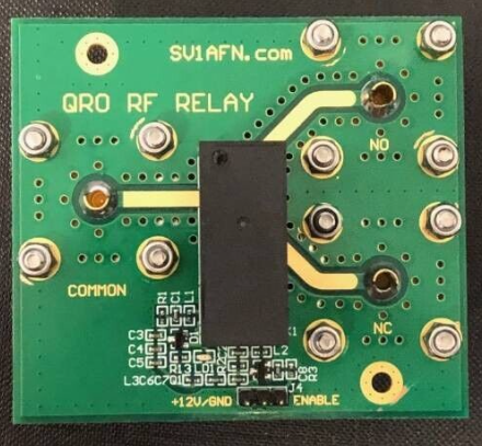
Prototype pcb diy
Step-by-Step Guide to Creating Your First Prototype PCB
Creating your first prototype printed circuit board (PCB) can be a rewarding experience, offering a tangible manifestation of your electronic design skills. To embark on this journey, it is essential to follow a structured approach, ensuring that each step is meticulously executed. This guide will walk you through the process, from initial design to the final assembly, providing a comprehensive understanding of the intricacies involved.
To begin with, the initial step in creating a prototype PCB is to conceptualize your design.
This involves defining the circuit’s functionality and determining the components required. Utilizing schematic capture software, such as Eagle or KiCad, can significantly streamline this process. These tools allow you to create a detailed schematic diagram, which serves as a blueprint for your PCB layout. It is crucial to ensure that all connections are accurately represented and that the components are correctly placed to avoid potential issues during the later stages.
Once the schematic is complete, the next phase involves designing the PCB layout.
This step translates the schematic into a physical representation, where the components are placed on the board, and the electrical connections are routed. During this stage, it is important to consider factors such as component placement, trace width, and signal integrity. Proper component placement can minimize signal interference and improve the overall performance of the circuit. Additionally, adhering to design rules and guidelines provided by PCB manufacturers can prevent common pitfalls and ensure manufacturability.
After finalizing the PCB layout, the design files need to be exported in a format suitable for manufacturing.
The most commonly used format is Gerber files, which contain information about the various layers of the PCB, including copper traces, solder mask, and silkscreen. It is advisable to perform a thorough design rule check (DRC) before exporting the files to identify any potential errors or violations. This step is critical as it helps in detecting issues that could compromise the functionality or manufacturability of the PCB.
With the Gerber files ready, the next step is to choose a PCB manufacturer.
Numerous online services offer PCB fabrication, catering to different requirements and budgets. When selecting a manufacturer, consider factors such as turnaround time, cost, and quality. Submitting your Gerber files to the chosen manufacturer will initiate the fabrication process, which typically involves several stages, including etching, drilling, and plating. The result is a bare PCB, ready for component assembly.
Component assembly is the subsequent phase, where the electronic components are soldered onto the PCB.
This can be done manually or using automated equipment, depending on the complexity and scale of the project. For beginners, manual soldering is often the preferred method. It is essential to follow proper soldering techniques to ensure reliable connections and avoid damaging the components or the PCB. Tools such as a soldering iron, solder wire, and flux are indispensable during this process.
Finally, once the components are assembled, it is imperative to test the prototype PCB to verify its functionality.
This involves powering up the circuit and performing various tests to ensure that it operates as intended. Debugging may be necessary if any issues are identified, requiring a systematic approach to isolate and rectify the problem. Successful testing marks the completion of your prototype PCB, ready for further development or production.
In conclusion, creating a prototype PCB involves a series of well-defined steps, each requiring careful attention to detail. From initial design to final testing, following a structured approach ensures a successful outcome. By adhering to best practices and leveraging appropriate tools, you can transform your electronic designs into functional prototypes, paving the way for innovation and development in the field of electronics.
Essential Tools and Materials for DIY PCB Prototyping
When embarking on the journey of DIY PCB prototyping, it is crucial to equip oneself with the essential tools and materials that will ensure a smooth and efficient process. The first and foremost requirement is a reliable computer with PCB design software. Programs such as Eagle, KiCad, or Altium Designer are indispensable for creating precise and functional PCB layouts. These software tools allow for the meticulous design of circuit schematics and the subsequent translation into a physical board layout.
Transitioning from the digital realm to the physical, a high-quality printer is necessary for transferring the PCB design onto a suitable medium.
Laser printers are often preferred due to their ability to produce sharp and clear images, which are essential for accurate etching. Alongside the printer, transparency film or glossy paper is required to print the PCB layout. This medium will later be used in the transfer process to the copper-clad board.
Speaking of copper-clad boards, these are the foundation upon which the PCB will be constructed.
These boards are typically made of fiberglass or other insulating materials, coated with a thin layer of copper. The copper layer is where the circuit paths will be etched, and it is vital to select a board that matches the size and specifications of your design.
To transfer the printed design onto the copper-clad board, a laminator or a clothes iron can be employed.
The heat from these devices will transfer the toner from the transparency film or glossy paper onto the copper surface. This step requires precision and care to ensure that the design adheres correctly without any smudges or misalignments.
Once the design is transferred, the next step involves etching the copper-clad board.
Ferric chloride is a commonly used etchant for this purpose. It is essential to handle this chemical with caution, using protective gloves and working in a well-ventilated area. The board is submerged in the ferric chloride solution, which will dissolve the exposed copper, leaving behind the desired circuit paths. After etching, the board must be thoroughly cleaned to remove any residual chemicals.
Drilling holes for component leads is another critical step in the PCB prototyping process.
A precision drill press or a handheld rotary tool with fine drill bits is necessary for this task. The holes must be accurately positioned and sized to accommodate the electronic components that will be mounted on the board.
Soldering is the final step in assembling the PCB.
A high-quality soldering iron with a fine tip is essential for making precise connections. Additionally, solder wire, flux, and a desoldering pump or wick are necessary tools for this stage. Proper soldering techniques are crucial to ensure reliable electrical connections and to avoid damaging the components or the board.
In conclusion, DIY PCB prototyping requires a combination of digital design tools, precise transfer and etching equipment, and meticulous assembly techniques. By investing in the right tools and materials, one can achieve professional-quality results in their PCB projects. Each step, from design to soldering, demands attention to detail and a methodical approach, ensuring that the final product meets the desired specifications and functions as intended.
Common Mistakes to Avoid in DIY PCB Prototyping
When embarking on the journey of DIY PCB prototyping, it is essential to be aware of common mistakes that can hinder the success of your project. One of the most frequent errors is inadequate planning. Before diving into the design and fabrication process, it is crucial to have a clear understanding of the circuit requirements, component specifications, and layout considerations. Failing to plan meticulously can lead to design flaws that are difficult to rectify later.
Another prevalent mistake is neglecting to double-check the schematic and layout.
Even minor errors in the schematic can result in significant issues during the prototyping phase. It is advisable to review the schematic multiple times and, if possible, have a peer or mentor examine it as well. Similarly, the layout should be scrutinized for potential problems such as overlapping traces, insufficient spacing between components, and incorrect pad sizes. Utilizing design rule checks (DRC) provided by PCB design software can help identify these issues early on.
Transitioning to the fabrication stage, improper handling of materials is a common pitfall.
For instance, using low-quality copper-clad boards or substandard etching chemicals can compromise the integrity of the PCB. It is essential to source high-quality materials and follow the recommended procedures for etching, drilling, and soldering. Additionally, maintaining a clean workspace and using appropriate safety gear can prevent contamination and ensure a safer working environment.
Furthermore, incorrect component placement and orientation are frequent mistakes that can lead to malfunctioning circuits.
It is vital to pay close attention to the polarity of components such as diodes and electrolytic capacitors, as reversing them can cause damage. Marking the PCB with clear indicators for component orientation can mitigate this risk. Moreover, using a multimeter to verify connections before soldering can save time and effort in troubleshooting later.
Another area where DIY enthusiasts often falter is in the soldering process.
Cold solder joints, excessive solder, and insufficient heat application are common issues that can affect the performance of the PCB. To avoid these problems, it is important to use a high-quality soldering iron with adjustable temperature settings and to practice proper soldering techniques. Ensuring that the soldering iron tip is clean and well-maintained can also improve the quality of the solder joints.
In addition, overlooking thermal management can lead to overheating and potential failure of the PCB.
Components such as voltage regulators and power transistors generate significant heat and require adequate cooling solutions. Incorporating heat sinks, thermal vias, and proper ventilation in the design can help dissipate heat effectively. It is also beneficial to consider the thermal properties of the PCB material and choose one that suits the application’s thermal requirements.
Finally, inadequate testing and validation can result in undetected issues that may surface during the operational phase.
It is essential to perform thorough testing of the PCB, including continuity checks, functional tests, and stress tests under different conditions. Documenting the test results and any anomalies can provide valuable insights for future iterations of the design.
In conclusion, avoiding these common mistakes in DIY PCB prototyping requires careful planning, meticulous attention to detail, and adherence to best practices throughout the design, fabrication, and testing stages. By being mindful of these potential pitfalls, hobbyists and professionals alike can enhance the reliability and performance of their PCB projects.
Top Software Options for Designing Prototype PCBs
Designing prototype printed circuit boards (PCBs) is a critical step in the development of electronic devices, and selecting the right software can significantly impact the efficiency and accuracy of this process. Several software options are available, each offering unique features tailored to different needs and levels of expertise. Understanding these options can help you make an informed decision, ensuring that your prototype PCB design is both effective and efficient.
One of the most popular software choices for designing prototype PCBs is Altium Designer.
Known for its comprehensive suite of tools, Altium Designer offers a robust environment for schematic capture, PCB layout, and even 3D modeling. Its advanced features, such as real-time collaboration and extensive component libraries, make it a preferred choice for professional engineers. However, its complexity and cost may be prohibitive for hobbyists or small startups.
Transitioning to a more accessible option, Eagle by Autodesk is another widely-used software in the PCB design community.
Eagle provides a balance between functionality and ease of use, making it suitable for both beginners and experienced designers. Its user-friendly interface and integration with Autodesk’s Fusion 360 allow for seamless transitions between electronic and mechanical design. Additionally, Eagle’s extensive online resources and community support make it an excellent choice for those new to PCB design.
For those seeking a free and open-source solution, KiCad is an outstanding option.
KiCad offers a comprehensive set of tools for schematic capture and PCB layout, rivaling many commercial software packages. Its open-source nature means that it is continually being improved by a dedicated community of developers and users. KiCad’s flexibility and lack of licensing fees make it particularly attractive for educational purposes and small-scale projects. However, it may require a steeper learning curve compared to more commercial options.
Another noteworthy mention is DipTrace, which provides a user-friendly interface and a range of features suitable for both simple and complex PCB designs.
DipTrace’s intuitive design environment, combined with its powerful component and pattern editors, allows for efficient and precise PCB creation. Its ability to import and export various file formats ensures compatibility with other design tools and manufacturing processes. While DipTrace offers a free version with limited capabilities, its full version is competitively priced, making it a viable option for small businesses and individual designers.
Moving on to a cloud-based solution, EasyEDA offers a unique approach to PCB design.
EasyEDA allows users to design, simulate, and share their projects entirely online, eliminating the need for software installation. Its integration with LCSC, a major electronic component supplier, streamlines the component selection and purchasing process. EasyEDA’s collaborative features enable multiple users to work on a project simultaneously, making it ideal for team-based projects. However, reliance on an internet connection and potential concerns about data security may be drawbacks for some users.
In conclusion, the choice of software for designing prototype PCBs depends on various factors, including the complexity of the project, budget constraints, and the user’s level of expertise. Altium Designer, Eagle, KiCad, DipTrace, and EasyEDA each offer distinct advantages and cater to different needs within the PCB design community. By carefully evaluating these options, designers can select the most suitable tool to bring their electronic innovations to life, ensuring a smooth and efficient design process.