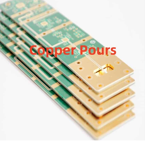
What is copper pour in pcb
Understanding Copper Pour in PCB Design
Copper pour, a fundamental concept in printed circuit board (PCB) design, refers to the practice of filling large, unused areas of a PCB with copper. This technique is employed for several reasons, each contributing to the overall functionality and efficiency of the PCB. To fully grasp the importance of copper pour, it is essential to understand its various applications and benefits within the realm of PCB design.
One of the primary reasons for utilizing copper pour is to enhance the electrical performance of the PCB.
By filling empty spaces with copper, designers can create a more stable ground plane, which is crucial for reducing electromagnetic interference (EMI). EMI can significantly affect the performance of electronic devices, leading to signal degradation and potential malfunction. A continuous ground plane, achieved through copper pour, helps to shield sensitive components from external noise and minimizes the risk of EMI, thereby ensuring the reliable operation of the device.
In addition to improving electrical performance, copper pour also plays a vital role in thermal management.
Electronic components generate heat during operation, and effective heat dissipation is necessary to prevent overheating and potential damage. Copper, being an excellent conductor of heat, aids in distributing thermal energy more evenly across the PCB. This distribution helps to maintain optimal operating temperatures for components, thereby extending their lifespan and enhancing the overall reliability of the device.
Moreover, copper pour contributes to the structural integrity of the PCB.
By adding additional copper to the board, designers can increase its mechanical strength, making it more resistant to bending and flexing. This added durability is particularly important in applications where the PCB may be subjected to physical stress or vibration. A robust PCB ensures that the connections between components remain intact, reducing the likelihood of failure due to mechanical stress.
Furthermore, copper pour can also lead to cost savings in the manufacturing process.
During the etching process, where unwanted copper is removed from the PCB, using copper pour reduces the amount of copper that needs to be etched away. This reduction in etching not only saves on material costs but also shortens the manufacturing time, leading to increased efficiency and lower production costs.
Transitioning to the design considerations, it is important to note that while copper pour offers numerous benefits, it must be implemented thoughtfully.
Designers need to ensure that the copper pour does not create unintended short circuits or interfere with signal integrity. Careful planning and adherence to design rules are essential to avoid potential issues. For instance, maintaining adequate spacing between copper pour areas and signal traces is crucial to prevent short circuits. Additionally, designers must consider the thermal expansion properties of copper to avoid stress on the PCB during temperature fluctuations.
In conclusion, copper pour is a valuable technique in PCB design that offers multiple advantages, including improved electrical performance, enhanced thermal management, increased mechanical strength, and cost savings in manufacturing. However, its implementation requires careful consideration to avoid potential pitfalls. By understanding and effectively utilizing copper pour, designers can create more reliable, efficient, and cost-effective PCBs, ultimately contributing to the success of electronic devices in various applications.
Benefits of Using Copper Pour in PCBs
Copper pour, a technique used in printed circuit board (PCB) design, involves filling large, unused areas of a PCB with copper. This practice is not merely for aesthetic purposes but serves several functional benefits that enhance the performance and reliability of the PCB. Understanding these benefits can provide valuable insights into why copper pour is a widely adopted practice in the electronics industry.
One of the primary advantages of using copper pour in PCBs is improved thermal management.
Electronic components generate heat during operation, and excessive heat can lead to component failure or reduced lifespan. Copper, known for its excellent thermal conductivity, helps dissipate heat more effectively.
By incorporating copper pour, the heat generated by components can be spread over a larger area, thereby reducing hotspots and maintaining a more uniform temperature across the PCB. This thermal regulation is crucial for high-power applications where heat dissipation is a significant concern.
In addition to thermal management, copper pour also enhances the electrical performance of the PCB.
It reduces the impedance of power and ground planes, which is particularly beneficial for high-frequency circuits. Lower impedance ensures that the power supply remains stable and minimizes voltage drops, which can otherwise lead to signal integrity issues. Furthermore, copper pour can act as a shield against electromagnetic interference (EMI). By providing a continuous ground plane, it helps in reducing the noise and crosstalk between different signal traces, thereby improving the overall signal quality.
Another significant benefit of copper pour is its contribution to the structural integrity of the PCB.
The additional copper layer adds mechanical strength, making the PCB more robust and less prone to warping or bending. This is especially important in applications where the PCB might be subjected to physical stress or varying environmental conditions. The enhanced durability ensures that the PCB can withstand the rigors of its intended application without compromising its functionality.
Moreover, copper pour can lead to cost savings in the manufacturing process.
By using copper pour, manufacturers can reduce the amount of etching required during the PCB fabrication process. This not only speeds up production but also minimizes the consumption of etching chemicals, making the process more environmentally friendly. Additionally, the reduced etching time can lower production costs, which is beneficial for both manufacturers and consumers.
Furthermore, copper pour can simplify the design process by providing a convenient way to connect multiple ground points.
Instead of routing individual ground traces, designers can use the copper pour as a common ground plane, which simplifies the layout and reduces the complexity of the PCB design. This can be particularly advantageous in multi-layer PCBs where space is at a premium, and efficient use of available area is critical.
In conclusion, the use of copper pour in PCBs offers a multitude of benefits that enhance the overall performance, reliability, and cost-effectiveness of the final product. Improved thermal management, enhanced electrical performance, increased structural integrity, cost savings in manufacturing, and simplified design are just a few of the advantages that make copper pour an indispensable technique in modern PCB design. As electronic devices continue to evolve and demand higher performance, the role of copper pour in ensuring the efficiency and reliability of PCBs will undoubtedly remain significant.
How to Implement Copper Pour in Your PCB Layout
Copper pour, also known as copper fill, is a technique used in printed circuit board (PCB) design to fill large areas of the board with copper. This practice not only helps in reducing the amount of etching solution required during the manufacturing process but also improves the electrical performance and thermal management of the PCB. Implementing copper pour in your PCB layout involves several steps, each requiring careful consideration to ensure optimal results.
To begin with, it is essential to understand the purpose of copper pour in your specific PCB design.
Copper pour can serve multiple functions, such as reducing electromagnetic interference (EMI), providing a low-impedance path for power and ground connections, and enhancing heat dissipation. By filling unused areas of the PCB with copper, you can create a more stable and efficient design. Therefore, the first step in implementing copper pour is to identify the areas where it will be most beneficial.
Once you have determined the areas for copper pour, the next step is to configure your PCB design software to create the copper pour.
Most PCB design tools, such as Altium Designer, Eagle, and KiCad, offer features to facilitate this process. Typically, you will need to select the layer on which you want to apply the copper pour, usually the top or bottom layer, and then define the boundaries of the pour area. It is crucial to ensure that the copper pour does not interfere with other components or traces on the board. To achieve this, you can set clearance rules that dictate the minimum distance between the copper pour and other elements.
After defining the boundaries and clearance rules, you can proceed to generate the copper pour.
This process involves filling the designated area with copper while adhering to the specified clearance rules. It is important to note that the copper pour should be connected to a net, typically the ground or power net, to ensure proper electrical functionality. In most design tools, you can assign the copper pour to a net by selecting the appropriate option in the software’s settings.
Once the copper pour is generated, it is essential to review the design to ensure that it meets all necessary requirements.
This includes verifying that the copper pour is properly connected to the intended net and that there are no unintended connections or shorts. Additionally, you should check for any potential issues related to thermal relief. Thermal relief refers to the practice of creating small gaps around vias and pads to facilitate soldering and prevent heat buildup. Most PCB design tools offer options to automatically generate thermal relief patterns, which can be adjusted based on your specific needs.
Finally, it is crucial to perform a thorough design rule check (DRC) to identify any potential issues before sending the PCB layout for manufacturing.
The DRC will help ensure that the copper pour and other design elements comply with the manufacturing constraints and industry standards. By addressing any issues identified during the DRC, you can minimize the risk of manufacturing defects and improve the overall quality of your PCB.
In conclusion, implementing copper pour in your PCB layout involves a series of well-defined steps, from identifying the areas for copper pour to configuring your design software and performing a thorough review. By carefully following these steps and considering the specific requirements of your design, you can effectively utilize copper pour to enhance the performance and reliability of your PCB.
Common Mistakes to Avoid with Copper Pour in PCB Design
Copper pour, a technique used in printed circuit board (PCB) design, involves filling large areas of the board with copper. This practice can enhance electrical performance, improve thermal management, and reduce manufacturing costs. However, improper implementation of copper pour can lead to several issues that compromise the functionality and reliability of the PCB. Understanding common mistakes and how to avoid them is crucial for achieving optimal results.
One frequent error in copper pour design is neglecting thermal reliefs.
Thermal reliefs are small traces that connect the copper pour to component pads, ensuring that heat can be effectively dissipated during soldering. Without these, the large copper areas can act as heat sinks, making it difficult to achieve proper solder joints. Consequently, components may not be securely attached, leading to potential failures. To avoid this, designers should always include thermal reliefs in their copper pour areas, ensuring a balance between heat dissipation and solderability.
Another common mistake is failing to consider the impact of copper pour on signal integrity.
Copper pour can create unintended capacitive coupling between traces, which can interfere with high-speed signals. This is particularly problematic in designs involving high-frequency components, where signal integrity is paramount. To mitigate this issue, designers should carefully plan the placement of copper pours, ensuring they do not overlap with critical signal traces. Additionally, using ground pours strategically can help shield sensitive signals from interference.
Inadequate clearance between copper pour and other elements on the PCB is another pitfall.
Insufficient spacing can lead to short circuits, especially if the copper pour encroaches on signal traces or component pads. This can result in erratic behavior or complete failure of the circuit. To prevent such issues, designers must adhere to the clearance guidelines specified by the PCB manufacturer. These guidelines typically account for the capabilities of the fabrication process and the requirements of the specific design.
Moreover, overlooking the importance of proper grounding can lead to significant problems.
Copper pour is often used to create ground planes, which are essential for reducing electromagnetic interference (EMI) and providing a stable reference voltage. However, if the ground plane is not properly connected to all relevant components, it can create ground loops or floating grounds, which can introduce noise and instability into the circuit. Ensuring that the ground plane is continuous and well-connected to all ground points is vital for maintaining the integrity of the PCB.
Additionally, designers sometimes make the mistake of not considering the thermal expansion properties of copper.
Copper expands and contracts with temperature changes, and if the copper pour is not properly segmented, it can cause mechanical stress on the PCB. This stress can lead to warping or even cracking of the board over time. To avoid this, designers should incorporate thermal relief cuts or slots in large copper areas, allowing for controlled expansion and contraction.
Lastly, improper use of copper pour can complicate the manufacturing process.
For instance, if the copper pour is too close to the edge of the PCB, it can cause issues during the routing and cutting stages of fabrication. This can result in damaged boards or increased production costs. Designers should ensure that copper pours are adequately set back from the edges and other critical areas to facilitate smooth manufacturing.
In conclusion, while copper pour is a valuable technique in PCB design, it requires careful consideration and implementation. By avoiding common mistakes such as neglecting thermal reliefs, compromising signal integrity, inadequate clearance, improper grounding, ignoring thermal expansion, and complicating the manufacturing process, designers can harness the benefits of copper pour without compromising the performance and reliability of their PCBs.