Summit pcb manufacturing
Innovations In Summit PCB Manufacturing
Summit PCB manufacturing has undergone significant advancements in recent years, driven by the relentless pursuit of innovation and efficiency. These innovations have not only enhanced the quality and reliability of printed circuit boards (PCBs) but have also streamlined the manufacturing process, making it more cost-effective and environmentally friendly.
One of the most notable advancements in Summit PCB manufacturing is the adoption of advanced materials.
Traditional PCBs were primarily made from materials like FR4, a composite of woven fiberglass cloth with an epoxy resin binder. However, the industry has seen a shift towards high-performance materials such as polyimide and Rogers laminates. These materials offer superior thermal stability, electrical performance, and mechanical strength, making them ideal for high-frequency and high-temperature applications. This transition has been pivotal in meeting the demands of modern electronic devices, which require more robust and reliable PCBs.
In addition to material advancements, the manufacturing process itself has seen remarkable improvements.
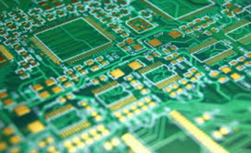
Automation and robotics have played a crucial role in enhancing precision and reducing human error. Automated optical inspection (AOI) systems, for instance, have become indispensable in detecting defects and ensuring the quality of PCBs. These systems use high-resolution cameras and sophisticated algorithms to inspect PCBs at various stages of production, identifying issues that might be missed by the human eye. This not only improves the overall quality of the final product but also reduces the time and cost associated with manual inspections.
Moreover, the integration of computer-aided design (CAD) and computer-aided manufacturing (CAM) software has revolutionized the design and production of PCBs.
These tools allow engineers to create highly detailed and accurate PCB layouts, which can then be directly translated into manufacturing instructions. This seamless transition from design to production minimizes errors and accelerates the development process. Furthermore, the use of simulation software enables engineers to test and optimize PCB designs before they are physically produced, ensuring that they meet all performance and reliability requirements.
Another significant innovation in Summit PCB manufacturing is the implementation of advanced fabrication techniques.
One such technique is laser direct imaging (LDI), which uses laser technology to directly transfer the PCB design onto the substrate. This method offers higher resolution and accuracy compared to traditional photolithography, allowing for the production of finer and more complex PCB patterns. Additionally, LDI reduces the need for masks and other consumables, making the process more environmentally friendly.
The industry has also seen a growing emphasis on sustainability and environmental responsibility.
Manufacturers are increasingly adopting green practices, such as using lead-free solder and reducing the use of hazardous chemicals. Recycling and waste management have become integral parts of the manufacturing process, with companies striving to minimize their environmental footprint. These efforts are not only driven by regulatory requirements but also by a growing awareness of the importance of sustainability in the electronics industry.
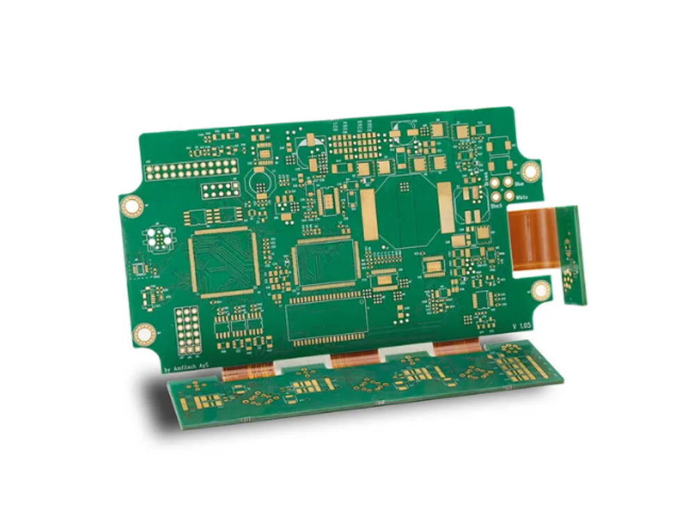
Furthermore, the rise of the Internet of Things (IoT) and the proliferation of connected devices have spurred the development of flexible and wearable PCBs.
These innovative PCBs are designed to be lightweight, bendable, and durable, making them suitable for a wide range of applications, from medical devices to smart textiles. The ability to integrate electronic components into flexible substrates opens up new possibilities for product design and functionality, driving further innovation in the industry.
In conclusion, Summit PCB manufacturing has made significant strides in recent years, thanks to advancements in materials, automation, design tools, fabrication techniques, and sustainability practices. These innovations have not only improved the quality and reliability of PCBs but have also made the manufacturing process more efficient and environmentally friendly. As the industry continues to evolve, it is poised to meet the growing demands of modern electronic devices and pave the way for future technological breakthroughs.
Quality Control Techniques In Summit PCB Production
In the realm of Summit PCB manufacturing, quality control techniques are paramount to ensuring the reliability and performance of printed circuit boards (PCBs). The intricate nature of PCBs, which serve as the backbone of modern electronic devices, necessitates rigorous quality control measures throughout the production process. These measures are designed to detect and rectify any defects that could compromise the functionality of the final product.
To begin with, the initial stage of quality control in Summit PCB production involves meticulous inspection of raw materials.
Ensuring that the substrates, copper foils, and other essential components meet stringent quality standards is crucial. Any deviation in the quality of these materials can lead to significant issues in the later stages of production. Therefore, suppliers are often required to provide certification and detailed specifications for the materials they deliver.
As the production process advances, automated optical inspection (AOI) systems play a critical role in maintaining quality.
These systems utilize high-resolution cameras and sophisticated algorithms to examine the PCBs for defects such as misalignments, soldering issues, and surface irregularities. By comparing the actual PCB to the intended design, AOI systems can quickly identify discrepancies and flag them for further review. This automated approach not only enhances accuracy but also significantly reduces the time required for inspection.
In addition to AOI, X-ray inspection is another vital technique employed in Summit PCB manufacturing.
This method is particularly useful for detecting hidden defects that are not visible to the naked eye or through optical inspection. For instance, X-ray inspection can reveal issues such as voids in solder joints, internal cracks, and misaligned layers within multilayer PCBs. By providing a non-destructive means of examining the internal structure of the boards, X-ray inspection ensures that even the most minute defects are identified and addressed.
Furthermore, electrical testing is an indispensable component of quality control in PCB production.
This involves subjecting the PCBs to a series of tests to verify their electrical integrity and functionality. Continuity tests, for example, check for open circuits and short circuits, ensuring that the electrical pathways are correctly established. Additionally, functional tests simulate the operating conditions of the final product to confirm that the PCB performs as expected. These tests are crucial for identifying any latent defects that could affect the performance of the electronic device in which the PCB will be installed.
Another important aspect of quality control is the implementation of stringent process controls during manufacturing.
This includes maintaining precise control over parameters such as temperature, humidity, and chemical concentrations during various stages of production. By closely monitoring these variables, manufacturers can prevent defects that arise from environmental fluctuations and ensure consistent quality across all batches of PCBs.
Moreover, continuous improvement practices are integral to the quality control framework in Summit PCB manufacturing.
This involves regularly reviewing and analyzing production data to identify trends and areas for improvement. By fostering a culture of continuous improvement, manufacturers can proactively address potential issues and enhance the overall quality of their products.
In conclusion, quality control techniques in Summit PCB production encompass a comprehensive array of measures designed to ensure the highest standards of reliability and performance. From the inspection of raw materials to advanced automated systems and rigorous electrical testing, each step in the process is meticulously managed to detect and rectify defects. Through the implementation of stringent process controls and a commitment to continuous improvement, Summit PCB manufacturers can deliver products that meet the exacting demands of modern electronic applications.
The Future Of Summit PCB Manufacturing Technology
The future of Summit PCB manufacturing technology is poised to revolutionize the electronics industry, driven by advancements in materials science, automation, and design methodologies. As the demand for more compact, efficient, and powerful electronic devices continues to grow, the need for innovative printed circuit board (PCB) solutions becomes increasingly critical. Summit PCB manufacturing, known for its high-quality and precision-engineered products, is at the forefront of this technological evolution.
One of the most significant advancements in Summit PCB manufacturing technology is the development of advanced materials.
Traditional PCBs are typically made from fiberglass-reinforced epoxy laminates, but new materials such as flexible polymers, ceramics, and even graphene are being explored. These materials offer superior electrical properties, thermal management, and mechanical flexibility, enabling the creation of more robust and versatile PCBs. For instance, flexible PCBs can be bent and folded without damaging the circuitry, making them ideal for wearable electronics and other applications where space is at a premium.
In addition to material innovations, automation is playing a crucial role in the future of Summit PCB manufacturing.
The integration of artificial intelligence (AI) and machine learning algorithms into the manufacturing process allows for real-time monitoring and optimization. Automated optical inspection (AOI) systems, for example, can detect defects and inconsistencies with unprecedented accuracy, ensuring that only the highest quality PCBs reach the market. Furthermore, robotic assembly lines can handle complex tasks with precision and speed, reducing production times and costs while maintaining stringent quality standards.
Another key area of development is in the design methodologies used in Summit PCB manufacturing.
Traditional design processes often involve multiple iterations and extensive manual labor, but modern computer-aided design (CAD) tools are streamlining this workflow. These tools enable engineers to create highly detailed and accurate PCB layouts, simulate their performance under various conditions, and make necessary adjustments before physical prototypes are produced. This not only accelerates the design cycle but also reduces the likelihood of errors and rework.
Moreover, the advent of additive manufacturing, or 3D printing, is set to transform Summit PCB manufacturing.
This technology allows for the creation of complex, multi-layered PCBs with intricate geometries that would be difficult or impossible to achieve using conventional methods. By depositing conductive and insulating materials layer by layer, 3D printing can produce PCBs with embedded components, reducing the need for external connections and enhancing overall performance. This approach also offers greater design flexibility and the potential for on-demand production, which can significantly reduce lead times and inventory costs.
Sustainability is another important consideration for the future of Summit PCB manufacturing.
As environmental concerns become more pressing, manufacturers are seeking ways to minimize waste and reduce the ecological footprint of their operations. This includes the development of eco-friendly materials, such as biodegradable substrates and lead-free solder, as well as the implementation of energy-efficient manufacturing processes. Recycling and reusing materials from end-of-life PCBs is also gaining traction, contributing to a more circular economy.
In conclusion, the future of Summit PCB manufacturing technology is characterized by a convergence of material innovations, automation, advanced design methodologies, additive manufacturing, and sustainability efforts. These advancements are not only enhancing the performance and reliability of PCBs but also driving efficiencies and reducing environmental impact. As the electronics industry continues to evolve, Summit PCB manufacturing is well-positioned to meet the growing demands for cutting-edge solutions, paving the way for a new era of technological progress.
Environmental Impact Of Summit PCB Manufacturing Practices
Summit PCB manufacturing, a critical component of the electronics industry, has seen significant advancements over the years. However, the environmental impact of these practices remains a pressing concern. The production of printed circuit boards (PCBs) involves various processes that can have detrimental effects on the environment if not managed properly. Understanding these impacts and the measures taken to mitigate them is essential for fostering sustainable manufacturing practices.
One of the primary environmental concerns associated with PCB manufacturing is the generation of hazardous waste
The etching process, which is used to create the intricate pathways on the boards, often involves the use of strong acids and bases. These chemicals, if not disposed of correctly, can lead to soil and water contamination. Additionally, the use of heavy metals such as lead, mercury, and cadmium in the soldering process poses significant risks. These metals are toxic and can accumulate in the environment, leading to long-term ecological damage.
Moreover, the energy consumption in PCB manufacturing is another critical factor.
The production process requires substantial amounts of electricity, particularly during the stages of drilling, plating, and lamination. This high energy demand contributes to the carbon footprint of the industry. Consequently, manufacturers are increasingly exploring renewable energy sources and energy-efficient technologies to reduce their environmental impact.
In addition to waste generation and energy consumption, water usage in PCB manufacturing is a significant concern.
The process involves multiple rinsing stages to clean the boards, which can lead to substantial water consumption. Furthermore, the wastewater generated often contains harmful chemicals and heavy metals. Proper treatment of this wastewater is crucial to prevent environmental contamination. Many manufacturers are now investing in advanced water treatment systems to ensure that the discharged water meets environmental standards.
Transitioning to more sustainable practices, Summit PCB manufacturing has seen a growing emphasis on the use of environmentally friendly materials.
For instance, the industry is gradually moving away from traditional lead-based solders to lead-free alternatives. These alternatives, such as tin-silver-copper alloys, are less harmful to the environment and human health. Additionally, there is a push towards using biodegradable and recyclable materials for PCB substrates, which can significantly reduce the environmental footprint of the manufacturing process.
Furthermore, the implementation of stringent environmental regulations has played a pivotal role in shaping the practices of PCB manufacturers.
Regulations such as the Restriction of Hazardous Substances (RoHS) directive and the Waste Electrical and Electronic Equipment (WEEE) directive in the European Union have set clear guidelines for reducing hazardous substances and promoting recycling. Compliance with these regulations not only helps in minimizing environmental impact but also ensures that manufacturers remain competitive in the global market.
In conclusion, while Summit PCB manufacturing is indispensable to the electronics industry, it is imperative to address its environmental impact. The generation of hazardous waste, high energy consumption, and significant water usage are critical issues that need to be managed effectively. By adopting sustainable practices, such as using environmentally friendly materials, investing in advanced treatment systems, and adhering to stringent regulations, the industry can mitigate its environmental footprint. As the demand for electronic devices continues to grow, it is essential for PCB manufacturers to prioritize sustainability and environmental responsibility in their operations.