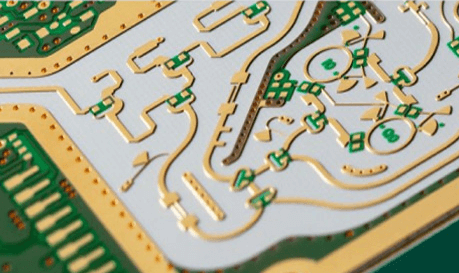
Rf pcb solder mask
Importance Of Solder Mask In Rf pcb solder mask
In the realm of Radio Frequency (RF) Printed Circuit Board (PCB) design, the solder mask plays a pivotal role in ensuring the functionality and reliability of the final product. The solder mask, a thin layer of polymer applied to the copper traces of a PCB, serves multiple critical purposes that are particularly significant in RF applications. Understanding the importance of the solder mask in RF PCB design requires a comprehensive examination of its functions and the unique challenges posed by high-frequency circuits.
Firstly, the solder mask acts as an insulator, preventing unintended electrical connections between adjacent conductive traces.
In RF PCB design, where signal integrity is paramount, even the slightest short circuit can lead to significant performance degradation. The solder mask ensures that the copper traces remain isolated, thereby maintaining the integrity of the signal paths. This isolation is crucial in high-frequency applications, where the proximity of conductive elements can lead to capacitive coupling and signal interference.
Moreover, the solder mask provides a protective barrier against environmental factors such as moisture, dust, and chemical contaminants.
RF circuits are often deployed in harsh environments where exposure to such elements can lead to corrosion and degradation of the copper traces. By shielding the conductive paths, the solder mask enhances the durability and longevity of the PCB, ensuring consistent performance over time. This protective function is particularly important in RF applications, where even minor degradation can result in significant signal loss or distortion.
In addition to its protective and insulating properties, the solder mask also plays a role in thermal management.
RF circuits can generate substantial amounts of heat, which, if not properly managed, can lead to thermal stress and potential failure of the PCB. The solder mask helps to dissipate heat by providing a uniform surface that facilitates the transfer of thermal energy away from the critical components. This thermal management capability is essential in maintaining the stability and reliability of RF circuits, especially in high-power applications.
Furthermore, the solder mask contributes to the manufacturability and assembly of RF PCBs.
During the soldering process, the mask prevents solder bridges from forming between adjacent pads, ensuring precise and reliable connections. This is particularly important in RF designs, where the density of components and traces can be quite high. The solder mask thus aids in achieving high-quality solder joints, which are essential for the optimal performance of RF circuits.
Transitioning to the aesthetic and identification aspects, the solder mask also provides a means for color-coding and labeling the PCB.
Different colors of solder masks can be used to distinguish between various layers or sections of the PCB, facilitating easier inspection and troubleshooting. Additionally, the mask can be printed with component identifiers and other markings, aiding in the assembly and maintenance processes.
In conclusion, the solder mask is an indispensable element in RF PCB design, offering a multitude of benefits that enhance the performance, reliability, and manufacturability of the final product. Its insulating properties prevent electrical shorts, its protective barrier shields against environmental damage, and its thermal management capabilities ensure stability under high-power conditions. Moreover, the solder mask aids in achieving precise solder joints and provides valuable identification and aesthetic functions. As RF technology continues to advance, the importance of the solder mask in ensuring the success of RF PCB designs cannot be overstated.
Common Challenges In Applying Solder Mask To RF PCBs
Applying solder mask to RF PCBs presents a unique set of challenges that require careful consideration and meticulous execution. One of the primary difficulties lies in the precision required for high-frequency circuits. RF PCBs often feature intricate designs with fine lines and spaces, necessitating a solder mask application that does not interfere with the signal integrity. Any misalignment or excess material can lead to signal loss or interference, which is detrimental to the performance of RF circuits.
Another significant challenge is the thermal management of RF PCBs.
These boards typically operate at higher frequencies, generating substantial heat. The solder mask must be able to withstand these elevated temperatures without degrading. This requires the use of specialized materials that can endure thermal cycling and maintain their properties over time. Additionally, the solder mask must not impede the heat dissipation process, which is crucial for maintaining the reliability and longevity of the PCB.
The choice of solder mask material is also critical.
Standard solder masks may not provide the necessary dielectric properties required for RF applications. A solder mask with inappropriate dielectric properties can alter the impedance of the circuit, leading to performance issues. Therefore, selecting a solder mask with the right dielectric constant and loss tangent is essential to ensure the proper functioning of the RF PCB.
Furthermore, the application process itself poses challenges.
Ensuring uniform coverage without defects such as bubbles, voids, or uneven thickness is vital. These defects can create points of weakness or areas where the solder mask does not adequately protect the underlying circuitry. Advanced techniques and equipment are often required to achieve the level of precision needed for RF PCBs. For instance, laser direct imaging (LDI) can be employed to enhance the accuracy of solder mask application, ensuring that even the most intricate designs are correctly masked.
Environmental factors also play a role in the application of solder masks to RF PCBs.
Contaminants such as dust, moisture, and oils can adversely affect the adhesion and performance of the solder mask. Maintaining a cleanroom environment during the application process is often necessary to mitigate these risks. Additionally, proper handling and storage of both the PCBs and solder mask materials are crucial to prevent contamination and ensure optimal results.
The curing process of the solder mask is another area where challenges can arise.
Inadequate curing can lead to poor adhesion and reduced protective qualities, while over-curing can cause brittleness and cracking. Achieving the right balance requires precise control of curing parameters such as temperature, time, and UV exposure. This often necessitates the use of sophisticated curing equipment and thorough process monitoring.
Lastly, the inspection and testing of the solder mask application are critical to identify and rectify any issues before the PCB is put into service.
Advanced inspection techniques, such as automated optical inspection (AOI) and X-ray inspection, can help detect defects that may not be visible to the naked eye. Ensuring that the solder mask meets all specified requirements and standards is essential for the reliability and performance of the RF PCB.
In conclusion, applying solder mask to RF PCBs involves navigating a complex array of challenges, from material selection and thermal management to precision application and environmental control. Each step in the process must be carefully managed to ensure that the final product meets the stringent requirements of high-frequency applications. By addressing these challenges with advanced techniques and meticulous attention to detail, manufacturers can produce RF PCBs that deliver optimal performance and reliability.
How Solder Mask Affects RF PCB Performance
In the realm of radio frequency (RF) printed circuit boards (PCBs), the solder mask plays a crucial role in determining the overall performance and reliability of the circuit. The solder mask, a thin layer of polymer applied to the surface of the PCB, serves multiple functions, including protecting the copper traces from oxidation, preventing solder bridges during assembly, and providing electrical insulation. However, its impact on RF PCB performance extends beyond these basic protective functions, influencing signal integrity, impedance control, and thermal management.
To begin with, the solder mask can significantly affect signal integrity in RF PCBs.
At high frequencies, even minor variations in the physical and electrical properties of the PCB materials can lead to signal degradation. The solder mask, being a dielectric material, introduces additional capacitance and can alter the impedance of the transmission lines. This alteration can cause signal reflections, leading to increased insertion loss and reduced signal strength. Therefore, careful selection of solder mask materials with low dielectric constants and loss tangents is essential to minimize these adverse effects and maintain signal integrity.
Moreover, the thickness and uniformity of the solder mask layer are critical factors in impedance control.
Impedance mismatches can result in signal reflections and loss, which are particularly detrimental in high-frequency applications. A non-uniform solder mask layer can create variations in the effective dielectric constant along the transmission line, leading to impedance discontinuities. Consequently, maintaining a consistent solder mask thickness and ensuring its uniform application are vital to achieving precise impedance control and optimizing RF performance.
In addition to signal integrity and impedance control, the solder mask also plays a role in thermal management.
RF circuits often generate significant amounts of heat, and efficient thermal dissipation is necessary to prevent overheating and ensure reliable operation. The solder mask can influence thermal conductivity and heat dissipation properties of the PCB. While the primary function of the solder mask is not thermal management, its presence can affect the thermal resistance of the PCB. Therefore, selecting solder mask materials with appropriate thermal properties and considering their impact on heat dissipation is important for maintaining optimal thermal performance in RF PCBs.
Furthermore, the solder mask can impact the manufacturability and reliability of RF PCBs.
During the assembly process, the solder mask helps prevent solder bridges between adjacent pads and traces, ensuring proper solder joint formation. However, improper application or defects in the solder mask can lead to issues such as solder mask slivers, voids, or misalignment, which can compromise the reliability of the PCB. Therefore, stringent quality control measures and adherence to industry standards are necessary to ensure the integrity of the solder mask and, consequently, the overall reliability of the RF PCB.
In conclusion, the solder mask is a critical component in RF PCBs, influencing various aspects of performance, including signal integrity, impedance control, thermal management, and reliability. Its dielectric properties, thickness, uniformity, and thermal characteristics all play a role in determining the overall performance of the RF circuit. Therefore, careful selection, application, and quality control of the solder mask are essential to optimize RF PCB performance and ensure reliable operation in high-frequency applications. By understanding and addressing the impact of the solder mask, designers and manufacturers can achieve superior RF PCB performance and meet the demanding requirements of modern RF applications.

Innovations In Solder Mask Materials For RF PCBs
In the realm of radio frequency (RF) printed circuit boards (PCBs), the solder mask plays a crucial role in ensuring the reliability and performance of the final product. Traditionally, solder masks have been used to protect the copper traces on PCBs from oxidation and to prevent solder bridges from forming during the soldering process. However, as the demand for higher frequency and more complex RF applications continues to grow, innovations in solder mask materials have become essential to meet these evolving requirements.
One of the primary challenges in RF PCB design is minimizing signal loss and interference.
Conventional solder masks, typically made from epoxy-based materials, can introduce unwanted dielectric properties that affect the signal integrity. To address this issue, researchers and manufacturers have been developing advanced solder mask materials with lower dielectric constants and loss tangents. These new materials help to reduce signal attenuation and maintain the integrity of high-frequency signals, which is critical for applications such as wireless communication, radar systems, and satellite technology.
In addition to improving dielectric properties, innovations in solder mask materials also focus on enhancing thermal management.
RF PCBs often operate at high power levels, generating significant amounts of heat. Effective thermal management is essential to prevent overheating and ensure the longevity of the components. Advanced solder mask materials with higher thermal conductivity have been developed to dissipate heat more efficiently. These materials help to maintain optimal operating temperatures, thereby improving the overall performance and reliability of RF PCBs.
Moreover, the mechanical properties of solder mask materials have also seen significant advancements.
RF PCBs are often subjected to harsh environmental conditions, including temperature fluctuations, humidity, and mechanical stress. To withstand these conditions, new solder mask formulations offer improved flexibility, adhesion, and resistance to cracking. These enhancements ensure that the solder mask remains intact and provides consistent protection throughout the lifespan of the PCB.
Another area of innovation is the development of environmentally friendly solder mask materials.
Traditional solder masks often contain volatile organic compounds (VOCs) and other hazardous substances that can be harmful to both human health and the environment. In response to increasing regulatory pressures and a growing emphasis on sustainability, manufacturers are now producing solder masks that are free from harmful chemicals and comply with environmental standards such as RoHS (Restriction of Hazardous Substances) and REACH (Registration, Evaluation, Authorization, and Restriction of Chemicals). These eco-friendly solder masks not only reduce the environmental impact but also ensure safer working conditions for those involved in the manufacturing process.
Furthermore, advancements in solder mask application techniques have also contributed to the overall performance of RF PCBs.
Precision application methods, such as laser direct imaging (LDI) and inkjet printing, allow for more accurate and consistent deposition of solder mask materials. These techniques enable the creation of finer features and tighter tolerances, which are essential for high-frequency applications. By improving the precision of solder mask application, manufacturers can achieve better control over the electrical and mechanical properties of the PCB.
In conclusion, the continuous innovations in solder mask materials for RF PCBs are driven by the need to enhance signal integrity, thermal management, mechanical durability, environmental sustainability, and application precision. As the demand for advanced RF applications continues to rise, these innovations will play a pivotal role in ensuring that RF PCBs meet the stringent performance and reliability requirements of modern technology. Through ongoing research and development, the industry is poised to deliver solder mask solutions that not only protect but also enhance the functionality of RF PCBs in increasingly complex and demanding applications.