Pcb x-out
Understanding PCB X-Out: What It Means and Why It Matters
Printed Circuit Boards (PCBs) are the backbone of modern electronic devices, serving as the foundation upon which electronic components are mounted and interconnected. In the manufacturing process of PCBs, the term “X-Out” frequently arises, and understanding its implications is crucial for both manufacturers and end-users.
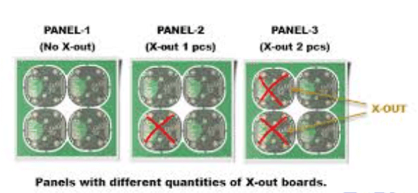
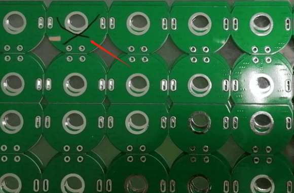
PCB X-Out refers to a board that has been identified as defective during the production process and is marked with an “X” to indicate its non-functional status. This practice is essential for maintaining quality control and ensuring that only fully functional boards are used in final products.
The identification of X-Out boards typically occurs during the inspection phase of PCB manufacturing.
After the boards are fabricated, they undergo rigorous testing to detect any defects that could compromise their performance. These defects can range from issues with the copper traces, solder mask, or silkscreen to more severe problems like short circuits or open circuits. When a defect is found, the board is marked with an “X” to signify that it does not meet the required standards. This marking is usually done with a permanent marker or a sticker, making it easily identifiable.
The presence of X-Out boards in a batch of PCBs has several implications.
Firstly, it affects the yield rate, which is a measure of the number of good boards produced versus the total number of boards manufactured. A high number of X-Outs indicates a lower yield rate, which can be a concern for manufacturers as it directly impacts production efficiency and cost. Consequently, manufacturers strive to minimize the occurrence of X-Outs through stringent quality control measures and continuous process improvements.
Moreover, the handling of X-Out boards is a critical aspect of inventory management.
Manufacturers must ensure that these defective boards are segregated from functional ones to prevent them from being inadvertently used in assembly processes. This segregation is vital because the use of an X-Out board in a final product can lead to device failure, resulting in customer dissatisfaction and potential warranty claims. Therefore, proper documentation and tracking of X-Out boards are essential to maintain the integrity of the supply chain.
In addition to affecting manufacturing processes, PCB X-Outs also have implications for cost management.
Defective boards represent wasted materials and labor, contributing to increased production costs. To mitigate these costs, manufacturers often analyze the root causes of defects and implement corrective actions. This may involve refining design specifications, improving fabrication techniques, or enhancing inspection protocols. By addressing the underlying issues that lead to X-Outs, manufacturers can reduce defect rates and improve overall production efficiency.
Furthermore, understanding PCB X-Outs is important for end-users, particularly those involved in the procurement and assembly of electronic components.
When sourcing PCBs, it is crucial to specify acceptable quality levels and ensure that suppliers adhere to these standards. This includes verifying that X-Out boards are properly identified and excluded from shipments. By doing so, end-users can avoid the risks associated with incorporating defective boards into their products, thereby ensuring reliability and performance.
In conclusion, PCB X-Outs play a significant role in the manufacturing and quality control of printed circuit boards.
They serve as a critical indicator of defects, impacting yield rates, inventory management, and cost efficiency. Both manufacturers and end-users must be vigilant in identifying, segregating, and addressing X-Out boards to maintain high standards of quality and reliability in electronic devices. Through continuous improvement and stringent quality control measures, the occurrence of X-Outs can be minimized, ultimately benefiting the entire supply chain.
The Impact of PCB X-Outs on Manufacturing Efficiency
Printed Circuit Boards (PCBs) are the backbone of modern electronic devices, serving as the foundation upon which electronic components are mounted and interconnected. In the manufacturing process of PCBs, the term “X-out” refers to a board that has been identified as defective or non-conforming to the required specifications. These X-out boards are typically marked with an “X” to indicate their status. The presence of PCB X-outs can have a significant impact on manufacturing efficiency, influencing various aspects of the production process.
To begin with, PCB X-outs can disrupt the flow of the manufacturing line.
When a defective board is identified, it must be removed from the production sequence, which can cause delays. This interruption necessitates additional handling and inspection, thereby increasing the time and labor required to maintain the production schedule. Consequently, the overall throughput of the manufacturing line is reduced, leading to potential bottlenecks and inefficiencies.
Moreover, the presence of X-out boards can affect the yield rate of the manufacturing process.
Yield rate, a critical metric in manufacturing, represents the percentage of non-defective products produced out of the total number of products manufactured. A high incidence of X-outs directly lowers the yield rate, indicating a higher proportion of defective boards. This not only reflects poorly on the quality control processes but also necessitates rework or replacement, further straining resources and increasing production costs.
In addition to affecting yield rates, PCB X-outs can also impact material utilization.
Each defective board represents wasted material, as the resources used to produce it cannot be recovered. This wastage is particularly significant in high-volume production environments where even a small percentage of defective boards can translate into substantial material losses. Efficient material utilization is crucial for cost-effective manufacturing, and the presence of X-outs undermines this objective.
Furthermore, the handling of X-out boards requires additional logistical considerations.
These boards must be segregated from conforming products to prevent them from inadvertently entering the supply chain. This segregation process involves additional steps such as labeling, storage, and documentation, all of which contribute to increased operational complexity. The need for meticulous tracking and management of X-out boards adds another layer of administrative burden, diverting attention and resources from core manufacturing activities.
Another aspect to consider is the potential impact on customer satisfaction.
Delivering high-quality products is paramount in maintaining customer trust and loyalty. The presence of X-out boards, if not properly managed, can lead to defective products reaching customers, resulting in returns, complaints, and potential damage to the manufacturer’s reputation. Ensuring that X-out boards are effectively identified and removed from the production line is essential in upholding product quality and customer satisfaction.
In conclusion, PCB X-outs have a multifaceted impact on manufacturing efficiency. They disrupt production flow, reduce yield rates, lead to material wastage, complicate logistical processes, and pose risks to customer satisfaction. Addressing the challenges posed by X-out boards requires robust quality control measures, efficient handling procedures, and continuous improvement efforts to minimize their occurrence. By effectively managing PCB X-outs, manufacturers can enhance their operational efficiency, reduce costs, and maintain high standards of product quality, ultimately contributing to a more streamlined and effective manufacturing process.
How to Minimize PCB X-Outs in Your Production Process
Printed Circuit Board (PCB) X-outs, which refer to defective boards within a panel, can significantly impact the efficiency and cost-effectiveness of your production process. Minimizing these X-outs is crucial for maintaining high-quality standards and ensuring the smooth operation of manufacturing lines. To achieve this, it is essential to implement a series of strategic measures that address various stages of the PCB production process.
First and foremost, the design phase plays a pivotal role in reducing PCB X-outs.
By adhering to design for manufacturability (DFM) principles, engineers can create layouts that are less prone to defects. This involves optimizing trace widths, spacing, and component placement to ensure that the design is robust and manufacturable. Additionally, conducting thorough design rule checks (DRC) and electrical rule checks (ERC) can help identify potential issues before they translate into physical defects.
Moving on to the material selection, choosing high-quality substrates and components is fundamental.
Inferior materials are more likely to result in defects such as delamination, warping, or poor solderability, which can lead to X-outs. Collaborating with reputable suppliers and conducting rigorous incoming quality control (IQC) inspections can help ensure that only top-grade materials are used in the production process.
The manufacturing process itself is another critical area where X-outs can be minimized.
Implementing stringent process controls and monitoring systems can help detect and address issues in real-time. For instance, automated optical inspection (AOI) and X-ray inspection systems can identify defects such as misalignments, solder bridges, and voids early in the production cycle. By catching these issues promptly, manufacturers can take corrective actions before they result in X-outs.
Furthermore, maintaining a clean and controlled manufacturing environment is essential.
Contaminants such as dust, moisture, and oils can cause defects during the PCB fabrication and assembly processes. Implementing cleanroom practices, such as using anti-static materials and ensuring proper ventilation, can help mitigate these risks. Regular equipment maintenance and calibration are also crucial to ensure that machinery operates within specified tolerances, thereby reducing the likelihood of defects.
In addition to these preventive measures, continuous training and education of the workforce are vital.
Skilled operators and technicians who are well-versed in best practices and quality standards are less likely to make errors that lead to X-outs. Providing ongoing training and fostering a culture of quality can empower employees to take ownership of their work and strive for excellence.
Moreover, implementing a robust quality management system (QMS) can provide a structured approach to minimizing X-outs.
A QMS that includes regular audits, root cause analysis, and corrective and preventive actions (CAPA) can help identify recurring issues and implement long-term solutions. By systematically addressing the root causes of defects, manufacturers can reduce the incidence of X-outs over time.
Finally, fostering strong communication and collaboration between design, manufacturing, and quality assurance teams is essential.
By working together and sharing insights, these teams can identify potential issues early and develop strategies to mitigate them. Regular cross-functional meetings and feedback loops can facilitate this collaboration and ensure that everyone is aligned towards the common goal of minimizing PCB X-outs.
In conclusion, minimizing PCB X-outs requires a comprehensive approach that spans the entire production process. By focusing on design optimization, material quality, process control, environmental cleanliness, workforce training, quality management, and cross-functional collaboration, manufacturers can significantly reduce the occurrence of X-outs. This not only enhances the overall quality of the PCBs but also improves production efficiency and cost-effectiveness, ultimately contributing to the success of the manufacturing operation.
Quality Control Strategies for Managing PCB X-Outs
Printed Circuit Boards (PCBs) are integral components in modern electronic devices, and their quality is paramount to the overall performance and reliability of the final product. One of the challenges faced in PCB manufacturing is the occurrence of PCB X-outs, which are defective boards identified during the production process. Managing these X-outs effectively is crucial to maintaining high standards of quality control. This article explores various strategies for managing PCB X-outs, ensuring that the manufacturing process remains efficient and cost-effective.
To begin with, it is essential to understand what PCB X-outs are.
X-outs are PCBs that have been marked as defective during the manufacturing process. These defects can arise from various issues such as misalignment, incomplete etching, or short circuits. Identifying these defective boards early in the production process is critical to prevent them from being assembled into final products, which could lead to malfunctions and customer dissatisfaction.
One of the primary strategies for managing PCB X-outs is implementing rigorous inspection protocols.
Automated Optical Inspection (AOI) systems are commonly used to detect defects in PCBs. These systems use high-resolution cameras and advanced algorithms to inspect each board for potential issues. By identifying defects early, manufacturers can segregate X-outs from good boards, ensuring that only high-quality PCBs proceed to the next stage of production.
In addition to AOI, manufacturers can employ Electrical Testing (ET) to further ensure the quality of PCBs.
ET involves applying electrical signals to the board and measuring the response to detect any discrepancies. This method is particularly effective in identifying issues such as open circuits or short circuits that may not be visible through optical inspection alone. By combining AOI and ET, manufacturers can achieve a higher level of accuracy in identifying X-outs.
Once X-outs have been identified, it is crucial to manage them effectively to minimize their impact on the production process.
One approach is to implement a rework and repair strategy. Depending on the nature of the defect, some X-outs can be repaired and brought up to the required quality standards. For instance, minor issues such as soldering defects can often be corrected through rework. However, it is important to assess the cost-effectiveness of rework, as some defects may be too severe to justify the expense and effort involved in repair.
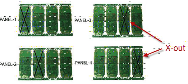
Another strategy for managing PCB X-outs is to optimize the panelization process.
Panelization involves grouping multiple PCBs on a single panel to streamline the manufacturing process. By carefully planning the layout of PCBs on the panel, manufacturers can minimize the impact of X-outs. For example, placing critical boards in positions that are less likely to be affected by defects can reduce the likelihood of X-outs affecting the overall yield. Additionally, incorporating redundant boards in the panel design can provide a buffer, allowing manufacturers to meet production targets even if some boards are marked as X-outs.
Furthermore, maintaining comprehensive records of X-outs and their causes can provide valuable insights for continuous improvement.
By analyzing data on defects, manufacturers can identify patterns and trends, enabling them to implement corrective actions to prevent similar issues in the future. This proactive approach not only improves the quality of PCBs but also enhances the overall efficiency of the manufacturing process.
In conclusion, managing PCB X-outs is a critical aspect of quality control in PCB manufacturing. By implementing rigorous inspection protocols, employing rework and repair strategies, optimizing panelization, and maintaining comprehensive records, manufacturers can effectively manage X-outs and ensure the production of high-quality PCBs. These strategies not only enhance the reliability of electronic devices but also contribute to the overall success and reputation of the manufacturing process.