Pcb laminate manufacturing process
Understanding The Basics Of PCB Laminate Materials
Printed Circuit Boards (PCBs) are the backbone of modern electronic devices, and their performance is heavily influenced by the materials used in their construction. Understanding the basics of PCB laminate materials is crucial for anyone involved in electronics design and manufacturing.
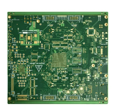
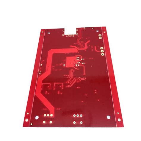
The laminate serves as the foundational structure of the PCB, providing mechanical support and electrical insulation between the conductive layers.
The manufacturing process of PCB laminates involves several critical steps, each contributing to the overall quality and functionality of the final product.
To begin with, the primary material used in PCB laminates is a composite of resin and reinforcing fibers.
The most common resin used is epoxy, known for its excellent electrical insulation properties and mechanical strength. The reinforcing fibers are typically made of woven glass fabric, which provides the necessary rigidity and dimensional stability. This combination of epoxy resin and glass fabric is often referred to as FR-4, the industry standard for PCB laminates due to its balanced properties and cost-effectiveness.
The manufacturing process starts with the impregnation of the glass fabric with the epoxy resin.
This step, known as prepregging, involves saturating the glass fabric with a partially cured epoxy resin. The prepreg sheets are then partially cured to a B-stage, where the resin is tacky but not fully hardened. This intermediate stage allows the prepreg sheets to be easily handled and layered during the subsequent lamination process.
Following the prepregging, the next step is the lamination process, where multiple layers of prepreg and copper foil are stacked together and subjected to heat and pressure.
The copper foil serves as the conductive layer, which will later be etched to form the circuit patterns. The stack-up of prepreg and copper foil is placed in a lamination press, where it is heated to a specific temperature and subjected to high pressure. This causes the epoxy resin to flow and fully cure, bonding the layers together into a solid laminate.
Once the lamination process is complete, the resulting laminate is cooled and removed from the press.
The next step involves drilling holes through the laminate to create vias, which are used to electrically connect different layers of the PCB. The drilled holes are then plated with copper to ensure reliable electrical connections. This step is critical, as any defects in the vias can lead to circuit failures.
After drilling and plating, the laminate undergoes a series of cleaning and surface preparation steps to ensure it is free of contaminants.
The surface of the laminate is then coated with a photoresist, a light-sensitive material that will be used to transfer the circuit pattern onto the copper foil. The photoresist-coated laminate is exposed to ultraviolet light through a photomask, which contains the desired circuit pattern. The exposed areas of the photoresist harden, while the unexposed areas remain soft and can be washed away, leaving the circuit pattern on the copper foil.
The final step in the PCB laminate manufacturing process is etching, where the exposed copper foil is chemically removed, leaving behind the desired circuit pattern.
The remaining photoresist is then stripped away, revealing the finished PCB laminate with its intricate network of conductive traces.
In conclusion, the manufacturing process of PCB laminates involves a series of meticulously controlled steps, each contributing to the overall performance and reliability of the final product. From the initial impregnation of glass fabric with epoxy resin to the final etching of the circuit pattern, every stage requires precision and attention to detail. Understanding these basics provides valuable insight into the complexities of PCB manufacturing and highlights the importance of high-quality materials and processes in the production of reliable electronic devices.
Step-By-Step Guide To PCB Laminate Manufacturing
The process of manufacturing PCB laminates is a meticulous and intricate procedure that requires precision and attention to detail. It begins with the selection of raw materials, which typically include a substrate material such as fiberglass or epoxy resin, and a conductive layer, usually copper foil. These materials are chosen for their electrical insulation properties and mechanical strength, which are essential for the performance and durability of the final product.
Once the raw materials are selected, the next step involves preparing the substrate.
This preparation includes cleaning and treating the surface to ensure it is free from contaminants and ready to bond with the copper foil. The substrate is then cut into sheets of the desired size, which will form the base of the PCB laminate.
Following the preparation of the substrate, the copper foil is laminated onto the substrate material.
This is achieved through a process called hot pressing, where the copper foil and substrate are subjected to high temperatures and pressure. The heat and pressure cause the adhesive layer between the copper and substrate to melt and bond them together, forming a single, cohesive laminate. This step is critical as it ensures the copper foil is securely attached to the substrate, providing a reliable conductive path for the electronic components that will be mounted on the PCB.
After the lamination process, the next step is to cool the laminate to room temperature.
This cooling process is essential to solidify the adhesive and ensure the laminate maintains its structural integrity. Once cooled, the laminate undergoes a series of inspections to check for any defects or irregularities. These inspections may include visual checks, as well as more advanced techniques such as X-ray or ultrasonic testing, to ensure the laminate meets the required specifications and quality standards.
Following the inspection, the laminate is then subjected to a process called drilling.
During this step, holes are drilled into the laminate at precise locations to accommodate the electronic components and interconnections that will be added later. The drilling process must be highly accurate, as any deviation can affect the performance and reliability of the final PCB.
Once the drilling is complete, the laminate undergoes a process called plating.
In this step, the drilled holes are coated with a thin layer of conductive material, typically copper, to create electrical connections between the different layers of the PCB. This plating process is crucial for ensuring the electrical continuity and functionality of the PCB.
After plating, the laminate is cleaned and prepared for the final step, which is the application of a protective coating. This coating, often referred to as a solder mask, is applied to the surface of the laminate to protect the copper traces from oxidation and environmental damage. The solder mask also helps to prevent short circuits by insulating the conductive paths on the PCB.
In conclusion, the manufacturing process of PCB laminates involves several critical steps, each requiring precision and attention to detail. From the selection of raw materials to the final application of the protective coating, every stage is essential to ensure the quality and reliability of the final product. By following this step-by-step guide, manufacturers can produce high-quality PCB laminates that meet the stringent demands of modern electronic devices.
Common Challenges In PCB Laminate Production And How To Overcome Them
In the intricate world of PCB laminate production, manufacturers often encounter a myriad of challenges that can impede the efficiency and quality of the final product. One of the most prevalent issues is the occurrence of delamination, where layers of the laminate separate due to inadequate bonding. This problem can be attributed to several factors, including improper curing temperatures, insufficient pressure during the lamination process, or contamination on the surface of the materials. To mitigate delamination, it is crucial to maintain stringent control over the lamination parameters and ensure that all surfaces are meticulously cleaned before the process begins.
Another significant challenge in PCB laminate production is the presence of voids and air bubbles within the laminate.
These imperfections can compromise the electrical performance and mechanical strength of the PCB. Voids often result from trapped air during the lamination process or from the outgassing of volatile components in the prepreg material. To address this issue, manufacturers can employ vacuum lamination techniques, which help to eliminate air pockets and ensure a more uniform and defect-free laminate. Additionally, selecting high-quality prepreg materials with low volatile content can further reduce the risk of void formation.
Thermal management is also a critical concern in PCB laminate production.
As electronic devices become more powerful and compact, the heat generated by the components can lead to thermal stress and potential failure of the PCB. Ensuring that the laminate material has adequate thermal conductivity and stability is essential to dissipate heat effectively. Manufacturers can overcome this challenge by incorporating materials with high thermal conductivity, such as metal cores or thermally conductive prepregs, into the laminate structure. Moreover, optimizing the design of the PCB to enhance heat dissipation, such as through the use of thermal vias and heat sinks, can further improve thermal management.
The dimensional stability of the laminate is another area where manufacturers often face difficulties.
Variations in temperature and humidity during the production process can cause the laminate to expand or contract, leading to misalignment of the layers and potential defects in the final PCB. To combat this issue, it is important to use materials with low coefficients of thermal expansion and to maintain a controlled environment during production. Implementing precise process controls and regular monitoring of environmental conditions can help to ensure that the laminate remains stable and within specified tolerances.
Furthermore, achieving consistent thickness and uniformity across the laminate is essential for the reliable performance of the PCB.
Variations in thickness can result from uneven pressure distribution during lamination or inconsistencies in the prepreg material. To address this challenge, manufacturers can utilize advanced lamination equipment that provides uniform pressure and temperature control. Additionally, conducting thorough inspections and quality checks at various stages of the production process can help to identify and rectify any deviations in thickness.
In conclusion, while PCB laminate production presents several challenges, manufacturers can overcome these obstacles through meticulous process control, the use of high-quality materials, and the implementation of advanced manufacturing techniques. By addressing issues such as delamination, void formation, thermal management, dimensional stability, and thickness uniformity, manufacturers can ensure the production of high-performance and reliable PCBs. Continuous improvement and innovation in the manufacturing process are essential to meet the evolving demands of the electronics industry and to maintain a competitive edge in the market.
Innovations In PCB Laminate Technology And Their Impact On Electronics
The manufacturing process of printed circuit board (PCB) laminates has undergone significant innovations in recent years, driven by the ever-increasing demand for more efficient, reliable, and compact electronic devices. These advancements have not only enhanced the performance and durability of PCBs but have also had a profound impact on the electronics industry as a whole. To understand the implications of these innovations, it is essential to delve into the specific technological advancements and their resultant benefits.
One of the most notable innovations in PCB laminate technology is the development of high-frequency laminates.
Traditional PCB laminates, typically made from materials such as FR-4, are suitable for a wide range of applications but fall short in high-frequency environments. High-frequency laminates, on the other hand, are designed to minimize signal loss and electromagnetic interference, making them ideal for applications in telecommunications, aerospace, and advanced computing. These laminates are often composed of materials like polytetrafluoroethylene (PTFE) and ceramic-filled composites, which offer superior electrical properties and thermal stability.
In addition to high-frequency laminates, the introduction of halogen-free laminates represents another significant advancement.
Traditional PCB laminates often contain halogenated flame retardants, which, while effective in preventing fires, pose environmental and health risks. Halogen-free laminates eliminate these concerns by using alternative flame-retardant materials that do not release toxic gases when exposed to high temperatures. This innovation aligns with the growing emphasis on sustainability and environmental responsibility in the electronics industry, as manufacturers strive to reduce their ecological footprint.
Moreover, the advent of flexible laminates has revolutionized the design and functionality of electronic devices.
Unlike rigid laminates, flexible laminates can bend and twist without compromising their electrical integrity, enabling the creation of flexible circuits. This flexibility is particularly advantageous in applications where space constraints and dynamic movement are critical factors, such as wearable technology, medical devices, and automotive electronics. The use of flexible laminates allows for more compact and lightweight designs, enhancing the overall user experience.
Another noteworthy innovation is the development of high thermal conductivity laminates.
As electronic devices become more powerful and compact, efficient heat dissipation becomes increasingly important to prevent overheating and ensure reliable performance. High thermal conductivity laminates, often made from materials like metal-core PCBs and thermally conductive polymers, facilitate the rapid transfer of heat away from critical components. This capability is crucial in high-power applications, such as LED lighting and power electronics, where thermal management is a key consideration.
Furthermore, advancements in PCB laminate manufacturing processes have led to improved precision and consistency.
Techniques such as laser direct imaging (LDI) and automated optical inspection (AOI) have enhanced the accuracy of patterning and defect detection, resulting in higher-quality laminates. These technologies enable manufacturers to produce PCBs with finer features and tighter tolerances, meeting the demands of modern electronic devices that require intricate and densely packed circuitry.
In conclusion, the innovations in PCB laminate technology have had a transformative impact on the electronics industry. High-frequency laminates, halogen-free laminates, flexible laminates, and high thermal conductivity laminates have each addressed specific challenges and requirements, paving the way for more advanced and reliable electronic devices. As the demand for smaller, faster, and more efficient electronics continues to grow, ongoing research and development in PCB laminate technology will undoubtedly play a crucial role in shaping the future of the industry. The integration of these advanced laminates into electronic designs not only enhances performance but also contributes to sustainability and environmental responsibility, reflecting the evolving priorities of the modern world.