High tech pcb
Innovations In High Tech PCB Manufacturing
Printed Circuit Boards (PCBs) are the backbone of modern electronic devices, serving as the foundation upon which all electronic components are mounted. The evolution of high tech PCB manufacturing has been marked by significant innovations that have enhanced the performance, reliability, and miniaturization of electronic devices. These advancements are driven by the increasing demand for more complex and compact electronic systems, which necessitate the development of cutting-edge manufacturing techniques.
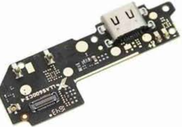
One of the most notable innovations in high tech PCB manufacturing is the advent of High-Density Interconnect (HDI) technology.
HDI PCBs are characterized by their higher wiring density per unit area compared to traditional PCBs. This is achieved through the use of microvias, finer lines and spaces, and thinner materials. The implementation of HDI technology allows for the creation of smaller, lighter, and more efficient electronic devices, which is particularly beneficial in industries such as consumer electronics, aerospace, and medical devices. The ability to pack more functionality into a smaller footprint is a key advantage of HDI PCBs, making them indispensable in the development of next-generation electronic products.
Another significant innovation is the use of advanced materials in PCB manufacturing.
Traditional PCBs are typically made from materials such as FR-4, a composite of woven fiberglass cloth with an epoxy resin binder. However, the limitations of these materials in terms of thermal performance and signal integrity have led to the exploration of alternative materials. High-frequency laminates, for instance, are designed to support high-speed signal transmission with minimal loss, making them ideal for applications in telecommunications and data centers. Additionally, the use of flexible and rigid-flex PCBs has gained traction, offering enhanced design flexibility and durability for applications that require dynamic bending and folding.
The integration of advanced manufacturing processes has also played a crucial role in the evolution of high tech PCBs.
Laser drilling, for example, enables the creation of extremely small and precise vias, which are essential for HDI PCBs. This process not only improves the accuracy and reliability of the vias but also reduces the overall manufacturing time. Similarly, the adoption of automated optical inspection (AOI) systems has revolutionized quality control in PCB manufacturing. AOI systems use high-resolution cameras and sophisticated algorithms to detect defects and ensure that each PCB meets stringent quality standards. This level of precision is critical in industries where even the smallest defect can lead to catastrophic failures.
Moreover, the push towards environmentally friendly manufacturing practices has led to the development of lead-free soldering techniques and the use of halogen-free materials.
These innovations not only reduce the environmental impact of PCB manufacturing but also comply with global regulations such as the Restriction of Hazardous Substances (RoHS) directive. The shift towards sustainable practices is a testament to the industry’s commitment to reducing its ecological footprint while maintaining high standards of performance and reliability.
In conclusion, the landscape of high tech PCB manufacturing is continually evolving, driven by the need for more compact, efficient, and reliable electronic devices. Innovations such as HDI technology, advanced materials, and cutting-edge manufacturing processes have significantly enhanced the capabilities of PCBs, enabling the development of sophisticated electronic systems. As the demand for high-performance electronics continues to grow, the PCB manufacturing industry will undoubtedly continue to innovate, pushing the boundaries of what is possible in electronic design and fabrication.
The Role Of High Tech PCBs In Modern Electronics
High tech printed circuit boards (PCBs) have become the backbone of modern electronics, playing a pivotal role in the functionality and efficiency of a wide array of devices. As technology continues to advance at a rapid pace, the demand for more sophisticated and reliable PCBs has surged, driving innovation in their design and manufacturing processes. These advanced PCBs are integral to the performance of contemporary electronic devices, from smartphones and laptops to medical equipment and automotive systems.
One of the primary reasons high tech PCBs are so crucial in modern electronics is their ability to support complex circuitry in a compact form.
As electronic devices become smaller and more powerful, the need for miniaturized components that can handle intricate electrical pathways has grown. High tech PCBs are designed to meet these requirements, offering multi-layered configurations that can accommodate a higher density of components. This capability not only enhances the performance of the devices but also contributes to their sleek and lightweight designs.
Moreover, the materials used in high tech PCBs are selected for their superior electrical, thermal, and mechanical properties.
Advanced substrates such as high-frequency laminates and flexible materials enable these PCBs to operate efficiently in demanding environments. For instance, in aerospace and defense applications, where reliability and durability are paramount, high tech PCBs must withstand extreme temperatures, vibrations, and other harsh conditions. The use of specialized materials ensures that these PCBs maintain their integrity and functionality under such stress.
In addition to material advancements, the manufacturing processes for high tech PCBs have also evolved significantly.
Techniques such as surface mount technology (SMT) and through-hole technology (THT) have been refined to improve the precision and reliability of PCB assembly. Furthermore, innovations in photolithography and etching processes have allowed for the creation of finer traces and more intricate circuit patterns. These advancements have enabled manufacturers to produce PCBs with higher performance capabilities and greater reliability, which are essential for the increasingly complex demands of modern electronics.
Another critical aspect of high tech PCBs is their role in enhancing the connectivity and communication capabilities of electronic devices.
With the proliferation of the Internet of Things (IoT) and the growing need for seamless data exchange, PCBs must support high-speed data transmission and robust connectivity. High tech PCBs are designed with advanced signal integrity features, such as controlled impedance and differential pair routing, to ensure that data is transmitted accurately and efficiently. This is particularly important in applications such as telecommunications and data centers, where the integrity of data transmission is crucial.
Furthermore, the integration of high tech PCBs in medical devices has revolutionized the healthcare industry.
These PCBs enable the development of sophisticated diagnostic and monitoring equipment, such as MRI machines, pacemakers, and wearable health monitors. The precision and reliability of high tech PCBs ensure that these medical devices operate accurately and consistently, ultimately improving patient outcomes and advancing medical research.
In conclusion, high tech PCBs are indispensable in the realm of modern electronics, driving innovation and enhancing the performance of a wide range of devices. Their ability to support complex circuitry, withstand demanding environments, and facilitate high-speed data transmission underscores their importance in today’s technology landscape. As electronic devices continue to evolve, the role of high tech PCBs will undoubtedly remain central to their development and success.
Advanced Materials Used In High Tech PCBs
High tech printed circuit boards (PCBs) are the backbone of modern electronic devices, enabling the complex functionalities that drive today’s technology. The evolution of PCBs has been marked by significant advancements in the materials used, which have been crucial in meeting the increasing demands for performance, reliability, and miniaturization. Advanced materials play a pivotal role in enhancing the capabilities of high tech PCBs, and understanding these materials is essential for appreciating the sophistication of contemporary electronics.
One of the most critical materials in high tech PCBs is the substrate, which provides the foundational support for the entire board.
Traditional PCBs often use FR-4, a composite material made of woven fiberglass cloth with an epoxy resin binder. However, high tech applications frequently require substrates with superior thermal and electrical properties. For instance, polyimide substrates are favored in high-frequency and high-temperature environments due to their excellent thermal stability and low dielectric constant. These properties make polyimide an ideal choice for aerospace, military, and advanced communication systems.
In addition to substrates, the conductive materials used in PCBs have also seen significant advancements.
Copper remains the primary choice for conductive traces due to its excellent electrical conductivity and relatively low cost. However, high tech PCBs often incorporate advanced copper alloys or even alternative metals like silver and gold to enhance performance. These materials offer lower resistance and better signal integrity, which are crucial for high-speed and high-frequency applications. Moreover, the use of advanced plating techniques, such as electroless nickel immersion gold (ENIG) and immersion silver, ensures superior surface finishes that improve solderability and corrosion resistance.
Another critical aspect of high tech PCBs is the dielectric materials used in the multilayer construction.
Dielectrics are insulating materials that separate the conductive layers and influence the board’s electrical performance. Advanced dielectrics, such as PTFE (polytetrafluoroethylene) and ceramic-filled composites, offer low dielectric constants and low loss tangents, making them suitable for high-frequency applications like RF and microwave circuits. These materials help minimize signal loss and ensure efficient transmission of high-speed signals, which is essential for modern communication devices and radar systems.
Thermal management is another area where advanced materials have made a significant impact.
High tech PCBs often operate in environments with substantial heat generation, necessitating efficient heat dissipation to maintain performance and reliability. Advanced thermal interface materials (TIMs), such as phase change materials and thermally conductive adhesives, are used to enhance heat transfer from critical components to heat sinks or other cooling mechanisms. Additionally, metal-core PCBs (MCPCBs) incorporate a metal layer, typically aluminum or copper, to provide superior thermal conductivity and mechanical strength, making them ideal for high-power LED applications and power electronics.
Furthermore, the miniaturization trend in electronics has driven the development of advanced materials that enable finer feature sizes and higher component densities.
High-density interconnect (HDI) PCBs utilize microvias, laser-drilled holes that connect multiple layers, and advanced laminates with improved dimensional stability. These materials and techniques allow for more compact and complex designs, supporting the ever-growing demand for smaller, more powerful electronic devices.
In conclusion, the advanced materials used in high tech PCBs are fundamental to the performance, reliability, and miniaturization of modern electronic devices. From substrates and conductive materials to dielectrics and thermal management solutions, these materials enable the sophisticated functionalities that define contemporary technology. As the demands on electronic devices continue to evolve, ongoing advancements in PCB materials will remain essential in pushing the boundaries of what is possible in the world of electronics.
Future Trends In High Tech PCB Design
The future of high-tech printed circuit board (PCB) design is poised for significant advancements, driven by the rapid evolution of technology and the increasing demand for more efficient, compact, and powerful electronic devices. As we look ahead, several key trends are emerging that promise to reshape the landscape of PCB design, offering new opportunities and challenges for engineers and manufacturers alike.
One of the most prominent trends in high-tech PCB design is the move towards miniaturization.
As electronic devices become smaller and more portable, the need for compact and densely packed PCBs has never been greater. This trend is particularly evident in the consumer electronics sector, where smartphones, wearables, and other portable gadgets require highly efficient use of space. To achieve this, designers are increasingly turning to advanced techniques such as high-density interconnect (HDI) technology, which allows for more components to be placed on a smaller board by using finer lines and spaces, smaller vias, and more layers.
In addition to miniaturization, the integration of multiple functionalities into a single PCB is another significant trend.
This is particularly relevant in the context of the Internet of Things (IoT), where devices need to perform a variety of tasks while maintaining a compact form factor. Multi-functional PCBs can incorporate sensors, processors, communication modules, and power management systems all on one board, reducing the need for multiple separate components and thereby enhancing efficiency and reliability.
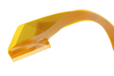
Another critical trend shaping the future of high-tech PCB design is the increasing use of flexible and rigid-flex PCBs.
These types of boards offer greater design versatility and can be used in applications where traditional rigid PCBs would be impractical. Flexible PCBs can bend and twist to fit into unconventional spaces, making them ideal for use in medical devices, automotive applications, and wearable technology. Rigid-flex PCBs combine the benefits of both rigid and flexible boards, providing robust performance while allowing for complex three-dimensional configurations.
Moreover, the rise of advanced materials is set to revolutionize PCB design.
Traditional PCBs are typically made from materials like FR4, but new materials such as liquid crystal polymer (LCP), polyimide, and metal-core PCBs are gaining traction. These advanced materials offer superior performance characteristics, including better thermal management, higher frequency capabilities, and improved mechanical strength. As electronic devices continue to demand higher performance, the adoption of these advanced materials is expected to grow.
Furthermore, the advent of artificial intelligence (AI) and machine learning (ML) is beginning to make its mark on PCB design.
AI and ML can be used to optimize the design process, predict potential issues, and suggest improvements, thereby reducing the time and cost associated with PCB development. These technologies can analyze vast amounts of data to identify patterns and trends that may not be immediately apparent to human designers, leading to more efficient and innovative designs.
Lastly, sustainability is becoming an increasingly important consideration in PCB design.
As the world grapples with environmental challenges, there is a growing emphasis on developing eco-friendly PCBs. This includes using recyclable materials, reducing waste during the manufacturing process, and designing boards that consume less power. Sustainable PCB design not only helps protect the environment but can also lead to cost savings and improved brand reputation.
In conclusion, the future of high-tech PCB design is characterized by miniaturization, multi-functionality, flexible and advanced materials, AI and ML integration, and a focus on sustainability. These trends are driving innovation and pushing the boundaries of what is possible in electronic design, promising a future where PCBs are more efficient, powerful, and environmentally friendly than ever before. As these trends continue to evolve, they will undoubtedly present new opportunities and challenges for designers and manufacturers, shaping the next generation of electronic devices.