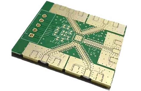
High frequency signal pcb design
Best Practices For High Frequency Signal PCB Layout
Designing printed circuit boards (PCBs) for high-frequency signals requires meticulous attention to detail and adherence to best practices to ensure signal integrity and minimize interference.
One of the fundamental principles in high-frequency PCB design is maintaining controlled impedance.
This involves carefully designing the trace width, spacing, and the dielectric material to ensure that the impedance remains consistent throughout the signal path. Variations in impedance can lead to signal reflections, which degrade the signal quality and can cause data errors.
Another critical aspect is the minimization of signal loss.
High-frequency signals are more susceptible to attenuation, which can be mitigated by using low-loss materials for the PCB substrate. Materials such as Rogers or Teflon are often preferred over traditional FR4 due to their lower dielectric constant and loss tangent. Additionally, ensuring that traces are as short and direct as possible helps to reduce signal loss and maintain signal integrity.
Ground planes play a pivotal role in high-frequency PCB design.
A continuous ground plane provides a return path for the signal, reducing the loop area and thereby minimizing electromagnetic interference (EMI). It is essential to avoid splitting the ground plane, as this can create impedance discontinuities and increase the risk of EMI. Furthermore, placing decoupling capacitors close to the power pins of integrated circuits helps to filter out high-frequency noise and stabilize the power supply.
Signal isolation is another best practice that cannot be overlooked.
High-frequency signals can easily couple with adjacent traces, leading to crosstalk and signal degradation. To mitigate this, designers should maintain adequate spacing between high-frequency traces and use differential pairs for signals that require high noise immunity. Differential pairs help to cancel out common-mode noise and improve signal integrity.
Via management is also crucial in high-frequency PCB design.
Vias introduce inductance and capacitance, which can affect the signal quality. To minimize these effects, it is advisable to use as few vias as possible and to ensure that they are properly back-drilled to remove any unused stubs. Additionally, using blind or buried vias can help to reduce the impact on signal integrity.
Thermal management is another important consideration.
High-frequency components often generate significant heat, which can affect their performance and reliability. Proper thermal management techniques, such as using thermal vias, heat sinks, and adequate copper pours, help to dissipate heat effectively and maintain the operational stability of the components.
Moreover, simulation and testing are indispensable in high-frequency PCB design.
Using simulation tools to model the PCB layout and predict signal behavior can help identify potential issues before the board is manufactured. Post-manufacturing testing, including time-domain reflectometry (TDR) and vector network analysis (VNA), provides valuable insights into the actual performance of the PCB and helps to verify that the design meets the required specifications.
In conclusion, designing PCBs for high-frequency signals demands a comprehensive understanding of various factors that influence signal integrity and performance. By adhering to best practices such as maintaining controlled impedance, minimizing signal loss, ensuring proper grounding, isolating signals, managing vias, and implementing effective thermal management, designers can create robust and reliable high-frequency PCBs. Additionally, leveraging simulation and testing tools further enhances the design process, ensuring that the final product meets the stringent requirements of high-frequency applications.
Material Selection For High Frequency PCB Design
When designing a high-frequency signal printed circuit board (PCB), the selection of materials is a critical factor that significantly influences the performance and reliability of the final product. The choice of substrate material, in particular, plays a pivotal role in determining the signal integrity, dielectric losses, and overall efficiency of the PCB. Therefore, understanding the properties and implications of various materials is essential for engineers and designers working in this domain.
To begin with, the dielectric constant (Dk) of the substrate material is a primary consideration.
High-frequency signals are highly sensitive to variations in the dielectric constant, which can lead to signal distortion and loss. Materials with a low and stable Dk are preferred because they minimize signal delay and ensure consistent signal propagation. Common materials such as FR-4, while cost-effective and widely used in low-frequency applications, may not be suitable for high-frequency designs due to their relatively high and variable Dk. Instead, materials like Rogers RO4000 series, which offer a low and stable dielectric constant, are often chosen for high-frequency applications.
In addition to the dielectric constant, the dissipation factor (Df) is another crucial parameter.
The dissipation factor measures the dielectric losses within the material, which directly affect the signal attenuation. Lower dissipation factors are desirable as they indicate lower energy loss and higher efficiency. High-frequency PCBs often employ materials like PTFE (Polytetrafluoroethylene) and ceramic-filled laminates, which exhibit low dissipation factors, thereby ensuring minimal signal loss and higher performance.
Thermal management is another aspect that cannot be overlooked in high-frequency PCB design. High-frequency signals can generate significant heat, and the substrate material must be capable of withstanding and dissipating this heat effectively. Materials with high thermal conductivity, such as ceramic-filled PTFE composites, are advantageous in such scenarios. These materials not only provide excellent thermal management but also maintain their electrical properties under varying thermal conditions, ensuring reliable performance.
Moreover, the coefficient of thermal expansion (CTE) is a vital consideration, especially in applications involving temperature fluctuations.
A mismatch in CTE between the substrate material and the copper traces can lead to mechanical stress and potential failure of the PCB. Therefore, selecting materials with a CTE that closely matches that of copper is essential to maintain the structural integrity of the PCB. Advanced materials like hydrocarbon ceramic laminates offer a balanced CTE, making them suitable for high-frequency applications.
Furthermore, the surface finish of the PCB material can impact signal integrity, particularly at high frequencies.
Surface finishes such as Electroless Nickel Immersion Gold (ENIG) and Immersion Silver are commonly used due to their excellent conductivity and smooth surface, which reduce signal reflection and loss. These finishes also provide good solderability and corrosion resistance, contributing to the overall durability of the PCB.
In conclusion, the selection of materials for high-frequency PCB design is a multifaceted process that requires careful consideration of various electrical, thermal, and mechanical properties. By choosing materials with low and stable dielectric constants, low dissipation factors, high thermal conductivity, and compatible CTE, designers can ensure optimal performance and reliability of high-frequency PCBs. Additionally, appropriate surface finishes further enhance signal integrity and durability, making them indispensable in the design of high-frequency signal PCBs. Through meticulous material selection, engineers can overcome the challenges associated with high-frequency signal transmission and achieve superior PCB performance.
Managing Signal Integrity In High Frequency PCBs
Managing signal integrity in high-frequency PCBs is a critical aspect of modern electronic design, as the performance and reliability of high-speed circuits depend heavily on maintaining the integrity of the signals they carry. As frequencies increase, the challenges associated with signal integrity become more pronounced, necessitating a comprehensive understanding of various factors that influence signal behavior. .
One of the primary considerations in high-frequency PCB design is the impedance control of transmission lines.
Impedance mismatches can lead to signal reflections, which degrade signal quality and can cause data errors. To mitigate this, designers must carefully calculate and control the impedance of traces, often employing techniques such as differential signaling and controlled impedance routing.
In addition to impedance control, managing crosstalk is essential for maintaining signal integrity.
Crosstalk occurs when a signal in one trace induces unwanted noise in an adjacent trace, which can be particularly problematic at high frequencies. To reduce crosstalk, designers can increase the spacing between traces, use ground planes to provide shielding, and employ differential pairs to cancel out noise. Furthermore, the use of proper grounding techniques is crucial in high-frequency PCB design. A well-designed ground plane can provide a low-impedance return path for signals, reducing the potential for ground loops and minimizing electromagnetic interference (EMI). Ensuring a continuous ground plane and avoiding split planes can significantly enhance signal integrity.
Another important aspect of managing signal integrity is the selection of appropriate materials for the PCB substrate.
The dielectric constant and loss tangent of the substrate material can affect signal propagation and attenuation. High-frequency designs often require low-loss materials to minimize signal degradation over long distances. Additionally, the choice of via structures and their placement can impact signal integrity. Vias introduce inductance and capacitance, which can distort high-frequency signals. To mitigate these effects, designers can use techniques such as back-drilling to remove unused via stubs and optimize via placement to minimize signal path discontinuities.
Moreover, the layout of components and traces plays a significant role in maintaining signal integrity.
Placing high-speed components close to each other and minimizing the length of high-frequency traces can reduce signal degradation. Careful routing of traces to avoid sharp bends and maintaining consistent trace widths can also help preserve signal quality. Signal integrity analysis tools, such as simulation software, can be invaluable in identifying potential issues and optimizing the PCB layout. These tools allow designers to model the behavior of high-frequency signals and predict the impact of various design choices on signal integrity. By simulating different scenarios, designers can make informed decisions to enhance the performance of their high-frequency PCBs.
Thermal management is another critical consideration in high-frequency PCB design.
High-speed circuits can generate significant heat, which can affect signal integrity and component reliability. Effective thermal management techniques, such as the use of thermal vias, heat sinks, and proper airflow, can help dissipate heat and maintain optimal operating conditions. In conclusion, managing signal integrity in high-frequency PCBs requires a multifaceted approach that encompasses impedance control, crosstalk reduction, proper grounding, material selection, via optimization, component placement, and thermal management. By addressing these factors, designers can ensure the reliable performance of high-speed circuits and meet the demanding requirements of modern electronic applications.
Techniques For Reducing EMI In High Frequency PCB Designs
In the realm of high frequency signal PCB design, managing electromagnetic interference (EMI) is paramount to ensuring optimal performance and reliability. EMI can significantly degrade the functionality of electronic circuits, leading to signal integrity issues and potential system failures. Therefore, employing effective techniques to mitigate EMI is crucial for engineers working on high frequency PCB designs.
One fundamental technique for reducing EMI is the careful layout of the PCB.
Proper component placement and routing are essential to minimize the coupling of noise between different parts of the circuit. For instance, placing high-speed components close to each other and routing high-frequency signals away from sensitive analog components can significantly reduce EMI. Additionally, maintaining short and direct signal paths helps to minimize the loop area, thereby reducing the potential for radiated emissions.
Another critical aspect of EMI reduction is the use of ground planes.
A continuous ground plane provides a low-impedance path for return currents, which helps to contain and dissipate EMI. By ensuring that the ground plane is uninterrupted and properly connected, designers can effectively shield sensitive components from electromagnetic noise. Moreover, employing multiple ground planes in a multilayer PCB design can further enhance EMI suppression by providing additional shielding and reducing the inductance of return paths.
In conjunction with ground planes, the strategic placement of decoupling capacitors is vital for EMI mitigation.
Decoupling capacitors act as local energy reservoirs, supplying transient currents to high-speed components and filtering out high-frequency noise. Placing these capacitors as close as possible to the power pins of integrated circuits helps to minimize the impedance of the power distribution network, thereby reducing EMI. Furthermore, using a combination of capacitors with different values can provide effective filtering across a wide range of frequencies.
Shielding is another effective technique for reducing EMI in high frequency PCB designs.
By enclosing sensitive components or entire sections of the PCB in conductive enclosures, designers can prevent electromagnetic radiation from escaping or entering the circuit. This is particularly important in applications where the PCB is exposed to external sources of EMI, such as wireless communication devices or industrial equipment. Shielding can be implemented using metal cans, conductive coatings, or even specially designed PCB layers that act as shields.
In addition to these techniques, careful consideration of signal integrity is essential for EMI reduction.
High-frequency signals are susceptible to reflections, crosstalk, and other forms of interference that can degrade signal quality. To mitigate these issues, designers should use controlled impedance traces, matched transmission lines, and proper termination techniques. Ensuring that signal traces are properly terminated and impedance-matched helps to minimize reflections and maintain signal integrity, thereby reducing EMI.
Moreover, the use of differential signaling can be highly effective in reducing EMI.
Differential pairs consist of two complementary signals that are routed together, with one signal being the inverse of the other. This configuration helps to cancel out common-mode noise, as any external interference affects both signals equally and is subsequently canceled out at the receiver. Differential signaling is particularly advantageous in high-speed data transmission, where maintaining signal integrity is critical.
In conclusion, reducing EMI in high frequency PCB designs requires a multifaceted approach that encompasses careful layout, effective grounding, strategic decoupling, shielding, and signal integrity considerations. By implementing these techniques, engineers can significantly enhance the performance and reliability of their high frequency circuits, ensuring that they operate efficiently in the presence of electromagnetic interference.