Flex pcb in altium
Designing Flex PCBs in Altium: Best Practices and Tips
Designing flexible printed circuit boards (PCBs) in Altium Designer requires a nuanced understanding of both the software’s capabilities and the unique characteristics of flex PCBs. As electronic devices continue to shrink in size while increasing in functionality, the demand for flexible PCBs has surged. These circuits offer the advantage of bending and folding, allowing for innovative designs in compact spaces. However, designing them involves specific considerations that differ from traditional rigid PCBs.
To begin with, understanding the material properties of flex PCBs is crucial.
Unlike rigid PCBs, which are typically made from fiberglass-reinforced epoxy laminate, flex PCBs use materials like polyimide, which provide the necessary flexibility. This material choice impacts the design rules and constraints that must be set in Altium. For instance, the bend radius is a critical parameter; it determines how much the board can flex without damaging the conductive traces. Altium Designer allows for the specification of these parameters, ensuring that the design adheres to the mechanical limitations of the materials used.
Transitioning from material considerations to layout strategies, it is essential to adopt best practices for trace routing.
In flex PCB design, traces should be routed perpendicular to the bend lines to minimize stress. Additionally, using curved traces instead of sharp angles can help distribute mechanical stress more evenly, reducing the risk of trace cracking. Altium Designer provides tools to facilitate these routing techniques, such as the ability to define and visualize bend areas, which helps in planning the trace paths effectively.
Moreover, the stack-up configuration in flex PCBs can be more complex than in rigid boards.
Flex circuits often involve multiple layers, including rigid-flex combinations where flexible and rigid sections are integrated into a single board. Altium Designer supports the creation of such complex stack-ups, allowing designers to define different material layers and their respective properties. This capability is particularly useful for ensuring that the electrical and mechanical characteristics of the board meet the design requirements.
Another critical aspect of designing flex PCBs in Altium is the use of design rule checks (DRCs).
These checks are vital for verifying that the design complies with manufacturing constraints and industry standards. Altium Designer offers customizable DRCs that can be tailored to the specific needs of flex PCB designs. For example, rules can be set to check for minimum trace width, spacing, and bend radius, ensuring that the design is manufacturable and reliable.
In addition to these technical considerations, collaboration and documentation are integral to the design process.
Altium Designer’s integrated environment facilitates collaboration among team members, allowing for seamless communication and data sharing. The software also provides robust documentation tools, enabling designers to generate comprehensive fabrication and assembly drawings. These documents are essential for communicating design intent to manufacturers, ensuring that the final product meets the desired specifications.
In conclusion, designing flex PCBs in Altium Designer involves a careful balance of material properties, layout strategies, stack-up configurations, and adherence to design rules. By leveraging Altium’s advanced features and adhering to best practices, designers can create flexible circuits that meet the demands of modern electronic applications. As technology continues to evolve, the ability to design efficient and reliable flex PCBs will remain a valuable skill in the electronics industry.
Advanced Layer Management for Flex PCBs in Altium
In the realm of modern electronics design, the demand for flexible printed circuit boards (PCBs) has surged, driven by the need for compact, lightweight, and versatile electronic devices. Altium Designer, a leading PCB design software, offers advanced tools for managing the complexities associated with flex PCB design. Understanding the intricacies of layer management in Altium is crucial for engineers aiming to harness the full potential of flex PCBs.
To begin with, flex PCBs differ significantly from their rigid counterparts, primarily due to their ability to bend and conform to various shapes.
This flexibility introduces unique challenges in layer management, as designers must account for mechanical stresses and potential signal integrity issues. Altium Designer addresses these challenges by providing a comprehensive suite of tools that facilitate precise control over layer stackups, material properties, and design rules.
One of the key features in Altium for managing flex PCBs is the Layer Stack Manager.
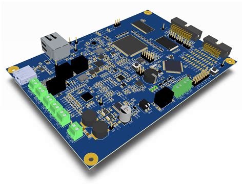
This tool allows designers to define and manipulate the various layers that constitute a flex PCB. By using the Layer Stack Manager, engineers can specify the number of conductive layers, dielectric materials, and adhesive layers, ensuring that the PCB meets both electrical and mechanical requirements. Moreover, Altium’s intuitive interface enables designers to visualize the layer stackup, making it easier to identify potential issues early in the design process.
In addition to defining the layer stack, Altium Designer offers advanced capabilities for managing the transition between rigid and flexible sections of a PCB.
This is particularly important in rigid-flex designs, where the PCB must maintain structural integrity while allowing for flexibility in certain areas. Altium’s design rules and constraints can be configured to ensure that the transition zones are optimized for both performance and manufacturability. By setting specific rules for trace width, spacing, and bend radius, designers can mitigate the risk of mechanical failure and signal degradation.
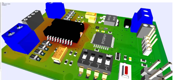
Furthermore, Altium Designer supports the use of 3D visualization tools, which are invaluable for flex PCB design.
These tools allow engineers to simulate the bending and folding of the PCB, providing insights into how the board will behave in real-world applications. By leveraging 3D visualization, designers can identify potential mechanical conflicts and make necessary adjustments before proceeding to fabrication. This not only reduces the likelihood of costly design iterations but also enhances the overall reliability of the final product.
Another critical aspect of flex PCB design in Altium is the management of impedance-controlled traces.
Given the potential for signal integrity issues in flexible circuits, maintaining consistent impedance is essential. Altium Designer’s impedance calculation tools enable designers to define and verify impedance-controlled traces, ensuring that high-speed signals are transmitted with minimal distortion. By integrating these calculations into the design process, engineers can achieve optimal performance in their flex PCB designs.
In conclusion, advanced layer management in Altium Designer is a pivotal component of successful flex PCB design.
By utilizing the software’s robust tools for layer stack management, transition zone optimization, 3D visualization, and impedance control, engineers can navigate the complexities of flex PCBs with confidence. As the demand for flexible electronics continues to grow, mastering these advanced techniques in Altium will be essential for designers seeking to create innovative and reliable electronic solutions.
Integrating Rigid-Flex Design in Altium: A Step-by-Step Guide
Integrating rigid-flex design in Altium Designer is a sophisticated process that requires a comprehensive understanding of both the software and the unique characteristics of rigid-flex PCBs. Rigid-flex PCBs combine the benefits of rigid and flexible circuits, offering enhanced design versatility, reduced weight, and improved reliability in complex electronic assemblies. As electronic devices continue to shrink in size while increasing in functionality, the demand for rigid-flex PCBs has grown significantly. Altium Designer, a leading PCB design software, provides robust tools to facilitate the design of these intricate circuits.
To begin integrating rigid-flex design in Altium, it is essential to first understand the structure of a rigid-flex PCB.
These boards consist of multiple layers, with rigid sections connected by flexible substrates. This configuration allows for three-dimensional assembly, which is particularly advantageous in applications where space is constrained. The design process in Altium starts with defining the stack-up, which involves specifying the number of layers, their materials, and thicknesses. This step is crucial as it lays the foundation for the entire design, ensuring that the mechanical and electrical properties meet the desired specifications.
Once the stack-up is defined, the next step is to create the board outline.
In Altium, this involves using the board shape editor to delineate the rigid and flexible regions. It is important to accurately define these areas, as they dictate the mechanical behavior of the PCB. Transitioning from rigid to flex regions requires careful consideration of bend radii and the placement of components to prevent mechanical stress and potential failure. Altium provides tools to simulate these transitions, allowing designers to visualize and adjust the board layout accordingly.
After establishing the board outline, the focus shifts to component placement and routing.
In rigid-flex design, component placement is more complex due to the need to accommodate both rigid and flexible areas. Altium’s 3D visualization capabilities are particularly useful at this stage, enabling designers to view the board from different angles and ensure that components are optimally placed. Routing in rigid-flex design also presents unique challenges, as traces must be carefully routed to avoid crossing the boundaries between rigid and flexible sections. Altium’s advanced routing tools assist in managing these complexities, providing features such as differential pair routing and length tuning to maintain signal integrity.
As the design progresses, it is imperative to conduct thorough design rule checks (DRCs) to identify potential issues.
Altium’s DRC engine is equipped to handle the intricacies of rigid-flex design, checking for violations such as minimum bend radius, trace width, and spacing constraints. These checks are vital to ensure that the design is manufacturable and meets industry standards.
Finally, once the design is complete, generating the necessary fabrication outputs is the last step.
Altium allows for the creation of detailed fabrication and assembly drawings, which are essential for communicating the design intent to manufacturers. These outputs include Gerber files, drill files, and a bill of materials, all of which are crucial for the successful production of the rigid-flex PCB.
In conclusion, integrating rigid-flex design in Altium Designer is a meticulous process that requires careful planning and execution. By leveraging Altium’s powerful tools and features, designers can create complex rigid-flex PCBs that meet the demands of modern electronic applications. The ability to seamlessly transition between rigid and flexible sections, combined with advanced simulation and verification capabilities, makes Altium an invaluable tool in the design of next-generation electronic devices.
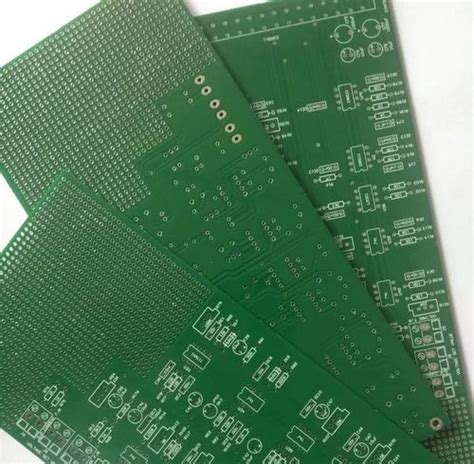
Troubleshooting Common Issues in Flex PCB Design with Altium
Designing flexible printed circuit boards (PCBs) in Altium can be a complex yet rewarding endeavor, offering a range of benefits such as reduced weight, increased flexibility, and enhanced durability. However, like any sophisticated design process, it is not without its challenges. Understanding and troubleshooting common issues that arise during the design phase can significantly enhance the efficiency and success of your project.
One of the most prevalent issues encountered in flex PCB design is the misalignment of layers.
This can occur due to inaccuracies in the design files or during the manufacturing process. To mitigate this, it is crucial to ensure that all layers are correctly aligned in the design software before proceeding to fabrication. Altium provides tools that allow designers to meticulously check and adjust layer alignment, ensuring that the final product meets the required specifications. Utilizing these tools effectively can prevent costly errors and rework.
Another common challenge is managing the bend radius of the flex PCB.
A bend radius that is too tight can lead to mechanical stress and potential failure of the circuit. Altium’s design rules can be configured to set minimum bend radii, helping designers to avoid these pitfalls. By adhering to these guidelines, designers can ensure that the flex PCB maintains its integrity and functionality over its intended lifespan. Additionally, simulating the bending process within Altium can provide valuable insights into how the PCB will perform in real-world applications.
Signal integrity is another critical aspect that can be compromised in flex PCB designs.
The flexible nature of these boards can introduce issues such as impedance mismatches and electromagnetic interference. To address these concerns, Altium offers advanced simulation tools that allow designers to analyze and optimize signal paths. By leveraging these tools, designers can identify potential problem areas and make necessary adjustments to maintain signal quality. Furthermore, careful consideration of trace width, spacing, and routing can significantly enhance signal integrity.
Thermal management is also a significant consideration in flex PCB design.
The materials used in flexible circuits often have different thermal properties compared to rigid boards, which can affect heat dissipation. Altium’s thermal analysis capabilities enable designers to evaluate the thermal performance of their designs and implement strategies to manage heat effectively. This might include the use of thermal vias, heat sinks, or other cooling mechanisms to ensure that the PCB operates within safe temperature limits.
Moreover, material selection plays a vital role in the success of a flex PCB design.
The choice of substrate and adhesive materials can impact the board’s flexibility, durability, and performance. Altium’s extensive library of materials allows designers to select the most appropriate options for their specific application. By carefully considering the material properties and their interaction with the design, potential issues can be minimized.
In conclusion, while designing flex PCBs in Altium presents unique challenges, understanding and addressing common issues can lead to successful outcomes. By leveraging Altium’s robust set of tools and features, designers can effectively troubleshoot and optimize their designs. From ensuring proper layer alignment and managing bend radii to maintaining signal integrity and thermal performance, each step is crucial in creating a reliable and efficient flex PCB. Through careful planning and execution, the complexities of flex PCB design can be navigated with confidence, resulting in innovative solutions that meet the demands of modern technology.
