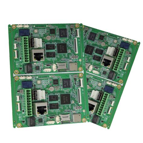
Pcb prototype manufacturing
Innovations In PCB Prototype Manufacturing Techniques
In recent years, the field of PCB (Printed Circuit Board) prototype manufacturing has witnessed significant innovations, driven by the increasing demand for more efficient, reliable, and cost-effective electronic components. As technology continues to advance at a rapid pace, manufacturers are constantly seeking new methods to enhance the design and production of PCBs, which are integral to the functionality of virtually all electronic devices. These innovations not only streamline the manufacturing process but also improve the performance and durability of the final products.
One of the most notable advancements in PCB prototype manufacturing is the adoption of additive manufacturing techniques, commonly known as 3D printing.
This technology allows for the creation of complex PCB designs with greater precision and flexibility than traditional subtractive methods. By building the circuit layer by layer, manufacturers can produce prototypes with intricate geometries that were previously difficult or impossible to achieve. Moreover, 3D printing reduces material waste and shortens production times, making it an attractive option for both small-scale and large-scale manufacturing.
In addition to 3D printing, the use of advanced materials has also revolutionized PCB prototype manufacturing.
High-performance substrates, such as polyimide and ceramic-based materials, offer superior thermal and electrical properties compared to conventional FR-4 materials. These advanced substrates enable the production of PCBs that can withstand higher temperatures and provide better signal integrity, which is crucial for high-frequency applications. Furthermore, the development of conductive inks and pastes has facilitated the creation of flexible and stretchable PCBs, opening up new possibilities for wearable electronics and other innovative applications.
Another significant innovation in PCB prototype manufacturing is the implementation of automated design and testing processes.
Computer-aided design (CAD) software has become increasingly sophisticated, allowing engineers to simulate and optimize PCB layouts before physical prototypes are produced. This not only reduces the likelihood of design errors but also accelerates the development cycle. Additionally, automated testing equipment can quickly identify defects and ensure that prototypes meet stringent quality standards, further enhancing the reliability of the final products.
The integration of artificial intelligence (AI) and machine learning into PCB prototype manufacturing is also gaining traction.
These technologies can analyze vast amounts of data to identify patterns and predict potential issues, enabling manufacturers to make informed decisions and improve production efficiency. For instance, AI algorithms can optimize component placement and routing, resulting in more compact and efficient PCB designs. Machine learning can also be used to enhance predictive maintenance, reducing downtime and extending the lifespan of manufacturing equipment.
Moreover, the trend towards miniaturization in electronics has spurred the development of innovative techniques for producing smaller and more densely packed PCBs.
Techniques such as laser direct structuring (LDS) and microvia drilling allow for the creation of high-density interconnect (HDI) PCBs, which are essential for modern electronic devices that require compact and lightweight components. These techniques enable the integration of more functionality into smaller spaces, meeting the demands of industries such as consumer electronics, automotive, and telecommunications.
In conclusion, the landscape of PCB prototype manufacturing is rapidly evolving, driven by technological advancements and the ever-growing demand for more sophisticated electronic devices. Innovations such as additive manufacturing, advanced materials, automated design and testing, AI integration, and miniaturization techniques are transforming the way PCBs are designed and produced. As these technologies continue to mature, they promise to further enhance the efficiency, performance, and reliability of PCB prototypes, paving the way for the next generation of electronic innovations.
The Role Of PCB Prototyping In Product Development
In the realm of product development, the significance of printed circuit board (PCB) prototyping cannot be overstated. As the backbone of modern electronic devices, PCBs serve as the foundation upon which electronic components are mounted and interconnected. The process of PCB prototyping plays a crucial role in transforming conceptual designs into tangible products, facilitating innovation and ensuring functionality before mass production. By understanding the role of PCB prototyping in product development, companies can enhance their design processes, reduce costs, and accelerate time-to-market.
To begin with, PCB prototyping allows engineers and designers to validate their designs in a real-world context.
During the initial stages of product development, ideas are often conceptualized through computer-aided design (CAD) software. While these digital models provide a comprehensive overview of the intended design, they cannot fully replicate the physical and electrical properties of a finished product. Prototyping bridges this gap by enabling the creation of a physical model that can be tested and evaluated. This hands-on approach allows for the identification of design flaws, such as incorrect component placement or inadequate trace routing, which might not be apparent in a virtual environment.
Moreover, PCB prototyping is instrumental in assessing the performance and reliability of a design.
By subjecting the prototype to various tests, such as thermal cycling, vibration analysis, and electrical testing, engineers can gather valuable data on how the PCB will perform under different conditions. This information is critical for making informed decisions about design modifications and improvements. Consequently, the iterative process of prototyping and testing helps in refining the design, ensuring that the final product meets the desired specifications and quality standards.
In addition to design validation and performance assessment, PCB prototyping also plays a pivotal role in cost management.
By identifying and rectifying potential issues early in the development process, companies can avoid costly redesigns and production delays. Furthermore, prototyping provides an opportunity to explore different materials and manufacturing techniques, allowing for cost optimization without compromising on quality. This proactive approach to cost management is particularly beneficial in competitive markets, where minimizing production expenses can significantly impact a product’s success.
Transitioning from design to production, PCB prototyping facilitates communication and collaboration among various stakeholders involved in product development.
Engineers, designers, manufacturers, and clients can all benefit from the tangible representation of the product that a prototype provides. It serves as a common reference point, enabling clearer communication of ideas and expectations. This collaborative environment fosters innovation and creativity, as stakeholders can provide feedback and suggestions based on their unique perspectives and expertise.
Finally, the role of PCB prototyping in product development extends to regulatory compliance and certification.
Many electronic products must adhere to specific industry standards and regulations before they can be marketed and sold. Prototyping allows companies to ensure that their designs comply with these requirements, reducing the risk of non-compliance and potential legal issues. By addressing regulatory concerns during the prototyping phase, companies can streamline the certification process and expedite product launch.
In conclusion, PCB prototyping is an indispensable component of product development, offering numerous benefits that extend beyond mere design validation. By enabling performance assessment, cost management, stakeholder collaboration, and regulatory compliance, prototyping paves the way for successful product innovation and commercialization. As technology continues to evolve, the importance of PCB prototyping in product development will only grow, underscoring its vital role in shaping the future of electronics.
Cost-Effective Strategies For PCB Prototype Production
In the realm of electronics, the development of printed circuit boards (PCBs) is a critical step in bringing innovative products to market. As the demand for more sophisticated and compact electronic devices grows, so does the need for efficient and cost-effective PCB prototype manufacturing. For companies and engineers, understanding the strategies to minimize costs while maintaining quality is essential.
One of the primary considerations in cost-effective PCB prototype production is the choice of materials.
Selecting the right substrate material can significantly impact both the performance and cost of the PCB. While high-frequency applications may require specialized materials, many prototypes can be effectively developed using standard FR-4 material, which offers a good balance between performance and cost. By carefully evaluating the requirements of the project, manufacturers can avoid unnecessary expenses associated with over-specifying materials.
Another crucial strategy involves optimizing the design for manufacturability (DFM).
This process entails designing the PCB layout in a way that simplifies the manufacturing process, thereby reducing costs. For instance, minimizing the number of layers in a PCB can lead to substantial savings, as each additional layer increases complexity and cost. Additionally, standardizing component sizes and using commonly available parts can further streamline production and reduce expenses. By collaborating closely with manufacturers during the design phase, engineers can identify potential cost-saving opportunities and address any manufacturability issues early on.
Furthermore, leveraging advanced software tools for design and simulation can also contribute to cost-effective PCB prototype production.
These tools allow engineers to simulate the performance of their designs before physical prototypes are produced, enabling them to identify and rectify potential issues early in the development process. This not only reduces the likelihood of costly rework but also accelerates the overall development timeline. Moreover, many of these software solutions offer features that assist in optimizing the layout for cost efficiency, such as automated component placement and routing.
In addition to design considerations, selecting the right manufacturing partner is pivotal in achieving cost-effective PCB prototype production.
Manufacturers with extensive experience and a proven track record in prototype development can offer valuable insights and guidance throughout the process. They often have established relationships with suppliers, which can lead to better pricing on materials and components. Furthermore, some manufacturers offer rapid prototyping services, which can significantly reduce lead times and allow for quicker iterations, ultimately saving both time and money.
Finally, adopting a lean manufacturing approach can further enhance cost-effectiveness.
This involves continuously analyzing and improving production processes to eliminate waste and increase efficiency. By implementing lean principles, manufacturers can reduce material waste, optimize labor utilization, and improve overall production flow. This not only lowers costs but also enhances the quality and reliability of the final product.
In conclusion, cost-effective PCB prototype production is achievable through a combination of strategic material selection, design optimization, advanced simulation tools, careful selection of manufacturing partners, and lean manufacturing practices. By integrating these strategies, companies can not only reduce costs but also improve the quality and speed of their prototype development, ultimately gaining a competitive edge in the fast-paced electronics market. As technology continues to evolve, staying informed about the latest advancements and best practices in PCB manufacturing will be crucial for success.
Challenges And Solutions In PCB Prototype Design
In the realm of electronics, the process of PCB prototype manufacturing is a critical step that bridges the gap between conceptual design and mass production. However, this phase is fraught with challenges that can significantly impact the efficiency and success of the final product. Understanding these challenges and exploring viable solutions is essential for engineers and designers aiming to optimize their prototype designs.
One of the primary challenges in PCB prototype manufacturing is the complexity of modern electronic designs.
As devices become more sophisticated, the demand for compact, multi-layered PCBs increases. This complexity can lead to issues such as signal integrity problems, electromagnetic interference, and thermal management challenges. To address these issues, designers must employ advanced simulation tools that allow for thorough testing and validation of the PCB design before physical prototyping begins. These tools can help identify potential problems early in the design process, reducing the likelihood of costly revisions later on.
Another significant challenge is the rapid pace of technological advancement, which often necessitates quick turnaround times for prototype development.
This urgency can lead to errors if not managed properly. To mitigate this, adopting an agile design approach can be beneficial. By breaking down the design process into smaller, manageable stages, teams can focus on iterative testing and refinement. This method not only enhances the quality of the prototype but also allows for more flexibility in accommodating changes and improvements.
Material selection also poses a challenge in PCB prototype manufacturing.
The choice of substrate material can greatly influence the performance and reliability of the PCB. Factors such as dielectric constant, thermal conductivity, and mechanical strength must be carefully considered. To navigate this complexity, collaboration with material suppliers can provide valuable insights into the latest materials and their properties. Additionally, leveraging industry standards and guidelines can aid in making informed decisions that align with the specific requirements of the project.
Cost considerations are another hurdle in the prototype design process.
The need to balance quality with budget constraints can be daunting. One solution is to employ design for manufacturability (DFM) principles, which focus on simplifying the design to reduce production costs without compromising functionality. By optimizing the layout and minimizing unnecessary components, designers can achieve a cost-effective prototype that meets performance expectations.
Furthermore, communication between design teams and manufacturing partners is crucial in overcoming challenges in PCB prototype manufacturing.
Miscommunication can lead to design errors, delays, and increased costs. Establishing clear communication channels and utilizing collaborative platforms can enhance coordination and ensure that all parties are aligned with the project goals. Regular meetings and updates can also facilitate the timely identification and resolution of potential issues.
In conclusion, while PCB prototype manufacturing presents several challenges, there are effective solutions that can be employed to navigate these obstacles. By leveraging advanced simulation tools, adopting agile design methodologies, carefully selecting materials, applying DFM principles, and fostering strong communication, designers can enhance the efficiency and success of their prototype designs. As the electronics industry continues to evolve, staying informed about emerging technologies and best practices will be essential for overcoming future challenges in PCB prototype manufacturing.