Hdr vs hdi PCB
Understanding The Differences: HDR Vs. HDI PCB Technologies
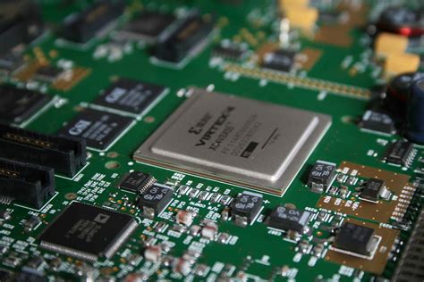
In the rapidly evolving world of electronics, printed circuit boards (PCBs) serve as the backbone of countless devices, from simple gadgets to complex computing systems. As technology advances, so do the methods and materials used in PCB manufacturing. Two such advancements are High-Density Interconnect (HDI) and High-Density Rigid (HDR) PCB technologies. Understanding the differences between these two technologies is crucial for engineers and designers aiming to optimize their products for performance, cost, and reliability.
To begin with, HDI PCBs are characterized by their ability to accommodate a higher density of components on a smaller board area.
This is achieved through the use of microvias, blind and buried vias, and fine lines and spaces. These features allow for more complex routing and greater functionality within a compact design. HDI technology is particularly beneficial in applications where space is at a premium, such as in smartphones, tablets, and other portable devices. The ability to integrate more components into a smaller area not only enhances the performance of the device but also reduces its overall size and weight.
In contrast, HDR PCBs focus on providing a robust and durable platform for electronic components.
These boards are typically used in applications where mechanical strength and reliability are paramount, such as in automotive, aerospace, and industrial equipment. HDR PCBs are designed to withstand harsh environmental conditions, including extreme temperatures, vibrations, and mechanical stress. The rigidity of these boards ensures that they maintain their structural integrity over time, making them ideal for use in critical applications where failure is not an option.
While both HDI and HDR PCBs offer distinct advantages, the choice between the two often depends on the specific requirements of the application.
For instance, if a project demands a compact design with high functionality, HDI technology may be the preferred choice. On the other hand, if the application requires a durable and reliable board capable of withstanding challenging conditions, HDR technology might be more suitable.
Moreover, the manufacturing processes for HDI and HDR PCBs also differ significantly.
HDI PCBs require advanced fabrication techniques, such as laser drilling for microvias and sequential lamination processes. These techniques can increase the complexity and cost of production. However, the benefits of HDI technology, such as reduced size and enhanced performance, often justify the additional expense. Conversely, HDR PCBs are typically manufactured using more traditional methods, which can be less costly and more straightforward. The focus here is on ensuring the board’s mechanical strength and reliability rather than maximizing component density.
In conclusion, both HDI and HDR PCB technologies offer unique benefits that cater to different needs within the electronics industry.
HDI PCBs excel in applications where space and performance are critical, while HDR PCBs provide the durability and reliability required for demanding environments. As technology continues to advance, the lines between these two technologies may blur, with future innovations potentially combining the best of both worlds. For now, understanding the differences between HDI and HDR PCBs allows engineers and designers to make informed decisions, ensuring that their products meet the necessary performance and reliability standards..
Benefits Of Using HDR Over HDI In PCB Design
In the realm of printed circuit board (PCB) design, the choice between High-Density Interconnect (HDI) and High-Density Rigid (HDR) technologies can significantly impact the performance, cost, and reliability of electronic devices. While both technologies offer unique advantages, HDR is increasingly being recognized for its superior benefits in certain applications. Understanding these benefits can guide engineers and designers in making informed decisions that optimize their designs for specific requirements.
To begin with, HDR technology offers enhanced mechanical stability compared to HDI.
This is primarily due to the rigid nature of HDR PCBs, which are constructed using robust materials that provide greater structural integrity. This characteristic is particularly advantageous in applications where the PCB is subjected to mechanical stress or vibration, such as in automotive or aerospace industries. The rigidity of HDR PCBs ensures that the components remain securely in place, reducing the risk of failure due to mechanical fatigue.
Moreover, HDR PCBs are known for their superior thermal management capabilities.
The materials used in HDR construction typically have better thermal conductivity, allowing for more efficient heat dissipation. This is crucial in high-power applications where excessive heat can lead to performance degradation or even damage to the components. By effectively managing heat, HDR PCBs contribute to the longevity and reliability of the electronic device, which is a critical consideration in industries where downtime can be costly.
In addition to mechanical and thermal advantages, HDR technology also offers improved electrical performance.
The design of HDR PCBs allows for shorter and more direct signal paths, which minimizes signal loss and reduces the potential for electromagnetic interference. This is particularly beneficial in high-frequency applications where signal integrity is paramount. The ability to maintain high signal quality ensures that the device operates efficiently and accurately, which is essential in precision-driven fields such as telecommunications and medical devices.
Furthermore, HDR PCBs provide greater design flexibility.
The rigid nature of these boards allows for the incorporation of complex multilayer designs, which can accommodate a higher density of components without compromising performance. This is especially useful in compact devices where space is at a premium. The ability to integrate more functionality into a smaller footprint not only enhances the device’s capabilities but also contributes to a more streamlined and aesthetically pleasing design.
While HDI technology is often lauded for its ability to support miniaturization and high component density, HDR offers a compelling alternative for applications where durability, thermal management, and electrical performance are prioritized. The choice between HDR and HDI ultimately depends on the specific requirements of the project, but the benefits of HDR make it an attractive option for many high-performance applications.
In conclusion, the advantages of using HDR over HDI in PCB design are manifold. From enhanced mechanical stability and superior thermal management to improved electrical performance and greater design flexibility, HDR technology provides a robust solution for demanding applications. As the electronics industry continues to evolve, the ability to leverage these benefits will be crucial in developing innovative and reliable products that meet the ever-increasing demands of modern technology. By carefully considering the unique advantages of HDR, designers can ensure that their PCB designs are optimized for success in a competitive and rapidly changing landscape.

Cost Implications: HDR Vs. HDI PCB Manufacturing
In the realm of printed circuit board (PCB) manufacturing, the choice between High-Density Interconnect (HDI) and High Dynamic Range (HDR) technologies can significantly impact the cost structure of a project. Understanding the cost implications of these two distinct approaches is crucial for manufacturers and designers aiming to optimize their production processes and budgets. While both HDR and HDI PCBs offer unique advantages, their cost considerations differ markedly, necessitating a thorough analysis to make informed decisions.
To begin with, HDI PCBs are renowned for their ability to accommodate more components in a smaller area, thanks to their advanced design techniques.
This capability is achieved through the use of microvias, blind and buried vias, and finer trace widths, which collectively allow for a higher density of interconnections. Consequently, HDI PCBs are particularly advantageous for applications requiring compact and lightweight designs, such as smartphones and other portable electronic devices. However, the intricate manufacturing processes involved in producing HDI PCBs often lead to higher production costs. The need for specialized equipment and materials, as well as the increased complexity of the design and fabrication stages, contribute to these elevated expenses. Moreover, the precision required in HDI manufacturing necessitates stringent quality control measures, further adding to the overall cost.
In contrast, HDR technology, primarily associated with display and imaging applications, focuses on enhancing the range of luminance and color depth in visual outputs.
While HDR is not directly related to PCB design, its integration into electronic devices can influence the cost of the overall system. The implementation of HDR capabilities often requires additional components, such as advanced display panels and specialized processing units, which can increase the bill of materials. Furthermore, the need for sophisticated software algorithms to manage HDR content adds another layer of complexity and cost. However, the benefits of HDR, including improved image quality and a more immersive user experience, can justify these additional expenses for applications where visual performance is paramount.
When comparing the cost implications of HDR and HDI PCBs, it is essential to consider the specific requirements and priorities of the project at hand.
For instance, if the primary goal is to achieve a compact and efficient design, the investment in HDI technology may be warranted despite its higher initial costs. On the other hand, if the focus is on delivering superior visual performance, the additional expenses associated with HDR integration may be justified. It is also worth noting that advancements in manufacturing technologies and economies of scale can influence the cost dynamics of both HDR and HDI PCBs over time. As these technologies continue to evolve, manufacturers may find opportunities to reduce costs through process optimization and increased production volumes.
In conclusion, the decision between HDR and HDI PCB manufacturing involves a careful evaluation of the cost implications associated with each technology. While HDI PCBs offer advantages in terms of miniaturization and component density, they come with higher production costs due to their complex manufacturing processes. Conversely, HDR technology enhances visual performance but may require additional investments in components and software. Ultimately, the choice between HDR and HDI should be guided by the specific needs and objectives of the project, taking into account both the immediate cost considerations and the long-term benefits each technology can provide.
Applications And Use Cases: When To Choose HDR Or HDI PCB
In the realm of printed circuit boards (PCBs), the choice between High-Density Interconnect (HDI) and High Dynamic Range (HDR) PCBs can significantly impact the performance and functionality of electronic devices. Understanding the applications and use cases for each type is crucial for engineers and designers aiming to optimize their products. While both HDR and HDI PCBs serve distinct purposes, their selection depends on the specific requirements of the project at hand.
To begin with, HDI PCBs are renowned for their ability to accommodate a higher density of components on a smaller board area.
This is achieved through the use of microvias, blind vias, and buried vias, which allow for more complex routing and layer interconnections. Consequently, HDI PCBs are particularly advantageous in applications where space is at a premium, such as in smartphones, tablets, and wearable devices. These applications demand compact designs without compromising on performance, making HDI PCBs an ideal choice. Furthermore, the increased interconnect density of HDI PCBs enhances signal integrity and reduces electromagnetic interference, which is critical in high-speed communication devices.
On the other hand, HDR PCBs are designed to handle a wide range of signal intensities, making them suitable for applications that require precise signal processing.
HDR technology is often employed in audio and video equipment, where the ability to accurately reproduce a broad spectrum of signals is paramount. For instance, in high-fidelity audio systems, HDR PCBs ensure that both the quietest and loudest sounds are captured and reproduced with clarity. Similarly, in video applications, HDR PCBs facilitate the display of images with greater contrast and detail, enhancing the overall viewing experience.
When deciding between HDR and HDI PCBs, it is essential to consider the specific demands of the application.
For projects that prioritize miniaturization and high component density, HDI PCBs are the preferred choice. Their ability to support complex designs and maintain signal integrity makes them indispensable in modern consumer electronics. Conversely, for applications that require superior signal processing capabilities, HDR PCBs are more suitable. Their proficiency in handling a wide dynamic range of signals makes them ideal for audio-visual equipment and other precision electronics.
Moreover, the decision between HDR and HDI PCBs can also be influenced by cost considerations.
HDI PCBs, due to their advanced manufacturing processes and materials, can be more expensive than traditional PCBs. However, the benefits they offer in terms of space-saving and performance often justify the additional cost. In contrast, HDR PCBs may not require the same level of complexity in manufacturing, potentially making them a more cost-effective option for applications where dynamic range is the primary concern.
In conclusion, the choice between HDR and HDI PCBs hinges on the specific requirements of the application. HDI PCBs excel in scenarios where high component density and compact design are crucial, while HDR PCBs are better suited for applications demanding precise signal processing. By carefully evaluating the needs of the project, engineers and designers can make informed decisions that enhance the performance and functionality of their electronic devices. As technology continues to evolve, the ability to select the appropriate PCB type will remain a critical factor in the success of electronic innovations.