Mastering BGA PCB Assembly: Techniques for Success
Key Takeaways
In the realm of BGA PCB assembly, mastering key techniques is instrumental for achieving optimal results. Understanding the fundamentals of BGA technology not only reinforces design decisions but also plays a critical role in ensuring that electronic devices perform reliably. When engaging in the pcb assembly process, it is vital to consider design factors such as pad size and layout, which directly impact solder quality. Utilizing appropriate soldering methods is equally important; techniques like reflow soldering can provide excellent thermal performance and create strong connections. Following the assembly, implementing rigorous inspection processes can help identify any potential issues during manufacturing—preventing costly failures later on. It’s essential to be adept at troubleshooting common challenges encountered in BGA assemblies, as this knowledge facilitates efficient problem resolution. Moreover, best practices for rework and repair of BGA components help maintain the integrity of the pcba while adhering to quality standards. Keeping an eye on emerging trends and innovations in the sector will also equip engineers with valuable insights for future projects, ensuring their skills remain relevant in a rapidly evolving industry.
Understanding BGA Technology: Fundamentals and Applications
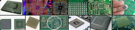
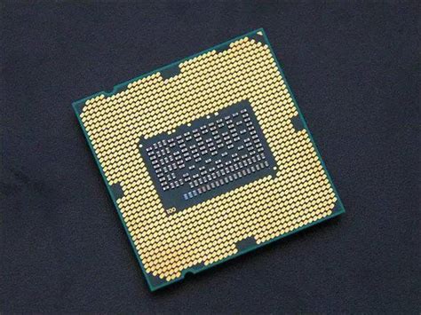
Ball Grid Array (BGA) technology has revolutionized the landscape of PCB assembly by providing a compact and efficient method for mounting integrated circuits (ICs) onto printed circuit boards (PCBs). The key innovation of BGA lies in its design, where the solder balls are located on the underside of the package, facilitating a high-density arrangement that minimizes space requirements without sacrificing electrical performance. This arrangement allows for better thermal management and signal integrity, essential factors for modern electronic devices.
In the context of pcba, understanding the fundamentals of BGA is crucial. The design considerations must include factors such as pad layout, thermal vias, and appropriate soldermask specifications. Engineers must also pay attention to substrate materials, which can significantly influence both performance and reliability. Numerous applications benefit from BGA technology, notably in sectors like telecommunications, automotive electronics, and consumer devices.
To adequately address these aspects, see the following table summarizing critical BGA characteristics:
| Characteristic | Description |
|---|---|
| Pitch Size | Typically ranges from 0.5 mm to 3 mm |
| Density | Allows for higher component density |
| Thermal Performance | Improved heat dissipation via solder balls |
| Mechanical Stress | Better resistance to mechanical stress due to more contact points |
Ultimately, a thorough comprehension of BGA fundamentals not only enhances the overall efficacy of pcba but also fosters innovation in electronic component design. Engineers who master these principles are well-equipped to handle complexities in BGA PCB assembly while ensuring high-quality and reliable connections in their end products.
Design Considerations for BGA PCB Assembly
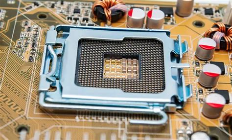
When undertaking BGA PCB assembly, several critical design considerations must be taken into account to ensure optimal performance and reliability of the final product. Ball Grid Arrays (BGAs), known for their excellent electrical performance, present unique challenges that demand careful planning during the design phase. One of the foremost aspects is the layer stack-up; ensuring that vias are properly placed to minimize signal integrity issues is essential. Additionally, the thermal management features of the PCB should be designed with heat dissipation in mind, as BGAs often generate significant heat during operation.
The footprint design for BGAs must adhere to specific industry standards to facilitate proper soldering and assembly. It is crucial to utilize appropriate pad dimensions and spacing to accommodate solder paste application adequately. Preventing bridging between balls is another vital factor, emphasizing the necessity of precise stencil design and solder paste deposition techniques.
Moreover, considering component placement is paramount in ensuring a successful assembly process. A well-defined path for pcba fabrication can reduce assembly time and decrease the risk of defects. It’s recommended to maintain sufficient clearance around BGA components for rework capability and inspection accessibility.
To optimize yield rates in the assembly process, designers should also incorporate features that facilitate testing after assembly, allowing for early detection of faults. Utilizing simulation tools during the design phase can help in identifying potential thermal or electrical issues before production begins.
“Implementing these considerations early in the design process can significantly enhance both yield and reliability.” Thus, understanding these factors not only contributes to more effective BGA PCB assembly but also fosters long-term trust in your electronic components’ functionality.
Soldering Methods: Techniques for Reliable Connections
In BGA PCB assembly, effective soldering methods are crucial for achieving reliable connections that ensure the longevity and performance of electronic components. One widely used technique is the reflow soldering process, where solder paste is applied to the pads of the PCB, and components are placed before being heated in a controlled environment. This allows the solder to melt and create a strong bond between the component leads and the board. Another popular method is wave soldering, which is particularly effective for through-hole components, providing a consistent application of solder. When working specifically with BGA packages, achieving uniform heating during reflow is essential, as uneven temperatures can lead to defects such as cold solder joints or insufficient wetting. Additionally, employing the correct stencil design for applying solder paste can greatly influence the quality of connections; too much or too little paste can compromise reliability. Utilizing advanced techniques such as thermal profiling helps monitor how heat moves through the PCB during the soldering process, ensuring that all areas reach optimal temperatures without exceeding tolerance levels that could damage components. Implementing these soldering methods systematically contributes to successful PCB assembly and enhances part integrity, ultimately leading to high-performance electronic devices.
Inspection Processes: Ensuring Quality and Performance
In the realm of BGA PCB assembly, effective inspection processes are crucial for guaranteeing the quality and performance of printed circuit board assemblies (PCBAs). These processes begin with thorough visual inspections, which can identify surface-level issues such as solder joint integrity and component placement. It’s vital to utilize automated optical inspection (AOI) systems, as they provide an efficient means to detect anomalies that might compromise performance. Furthermore, employing X-ray inspection is essential for validating solder joints beneath the BGA components, where traditional visual methods may fall short.
Once initial inspections are complete, it is important to follow up with functional testing to ensure that the PCBA operates as intended under real-world conditions. During this stage, electrical tests can uncover any hidden defects that manifest only during operational stress. Combining these techniques helps build a comprehensive inspection protocol, ensuring that all aspects of the assembly are scrutinized.
Quality control is not merely about detecting defects; it’s also about analyzing trends and implementing corrective actions for any recurring issues. Regularly reviewing inspection data aids in refining the overall PCBA process, making it more efficient and less prone to errors in subsequent productions. Adopting these rigorous inspection practices will not only enhance the reliability of BGA assemblies but also bolster client confidence in the final product. Ultimately, rigorous inspection processes that prioritize quality will yield PCBAs capable of meeting the increasing demands of high-performance electronics applications.
Troubleshooting Common BGA Assembly Issues
In the realm of BGA PCB assembly, encountering challenges is not uncommon. Understanding these issues is crucial for ensuring the reliability and performance of the assembled Printed Circuit Boards (PCBs). One frequent problem arises from insufficient solder joint formation, which can lead to poor electrical connectivity and component failure. During the pcba process, inadequate heat distribution may prevent proper solder melting, resulting in cold solder joints. It is essential to monitor the reflow temperature closely and adjust it based on the materials being used.
Another common issue is misalignment of BGA components, which can occur during placement or reflow soldering. To address this, operators should ensure accurate alignment alignment mechanisms are in place when positioning components on the board. Moreover, employing a robust inspection process post-assembly can help to identify misalignments early on.
Additionally, micro-cracks may develop during thermal cycling or mechanical stress, affecting long-term reliability. Therefore, incorporating rigorous testing methods, such as X-ray inspection or automated optical inspection (AOI), can greatly assist in identifying such defects before pcba completion.
Lastly, solder mask issues can contribute to assembly failures if there are contaminants or improper mask application that block solder adhesion. Frequent checks of the solder mask quality and proper cleaning procedures prior to assembly are advisable for reducing this risk.
By understanding these common issues and implementing corrective measures efficiently, manufacturers can significantly enhance their BGA PCB assembly processes and produce high-performance electronic components that meet market demands.
Best Practices for Rework and Repair of BGA Components
When it comes to BGA PCB assembly, the rework and repair of BGA components can be particularly challenging due to their complex nature and fine pitch. However, adhering to a set of best practices can significantly enhance success rates. First and foremost, proper analysis is crucial; assessing the failure mode can guide the rework strategy effectively. Be sure to use appropriate tools, such as hot air rework stations or infrared heaters, which enable precise heat application without damaging surrounding components. Additionally, employing solder paste that supports BGA repairs ensures reliable connections are made during the pcb assembly process.
It’s also essential to keep a close eye on the integrity of the printed circuit board during rework; using low-temperature solder can help minimize thermal stress. Following this, performing thorough inspections using X-ray machines or other suitable techniques allows for the detection of hidden connections often associated with BGA assemblies. Finally, when it comes to testing repaired boards, ensure that you utilize effective methods such as in-circuit testing (ICT) or functional testing to verify that all repairs are successful and maintain the reliability expected from high-quality pcba processes. By incorporating these practices into your BGA assembly work, you will not only facilitate successful repairs but also enhance the overall performance and reliability of your electronic components.
The Future of BGA PCB Assembly: Trends and Innovations
As technology progresses, the landscape of BGA PCB assembly is constantly evolving, driven by innovations that promise to enhance both efficiency and reliability in pcba processes. With the surge in demand for high-performance electronic devices, manufacturers are increasingly adopting advanced materials and techniques to improve the functionality of BGA packages. Notably, the integration of innovative lead-free soldering methods addresses environmental concerns while ensuring robust connections. Moreover, automated inspection processes are becoming more sophisticated, utilizing artificial intelligence and machine learning to detect defects quicker and more accurately, which significantly reduces downtime and enhances overall pcb assembly quality. Another key trend is the emphasis on thermal management solutions within BGA designs—ensuring that power-dense components can operate efficiently without overheating. Furthermore, industry leaders are exploring flexible and printed electronic technologies that could dramatically reshape the future landscape of pcba, offering new potentials for miniaturization and function integration. Embracing these trends not only leads to optimized production processes but also ensures that manufacturers can meet ever-growing consumer expectations for performance and reliability in their electronic products. As we look forward, staying attuned to these innovations will be crucial in mastering BGA PCB assembly practices effectively.
Conclusion
In summary, mastering BGA PCB assembly requires a thorough understanding of various critical aspects that contribute to the overall effectiveness and reliability of the final product. From the initial design phase to choosing appropriate soldering methods, each step is pivotal in ensuring a successful pcb assembly. Implementing comprehensive inspection processes allows for the identification of potential issues early on, facilitating corrective measures that enhance performance and longevity. Furthermore, being prepared to troubleshoot common challenges in pcba can save significant time and resources in production. Adhering to best practices not only promotes quality but also eases rework and repair efforts for BGA components when necessary. As technology continues to evolve, staying informed about the latest trends and innovations in BGA PCB assembly will empower engineers and technicians alike, ensuring they are equipped for future challenges in the electronic manufacturing landscape.
FAQs
What is BGA PCB assembly?
BGA PCB assembly, or Ball Grid Array PCB Assembly, is a process used for mounting surface-mount electronic components on a printed circuit board (PCB). It involves placing BGA packages, which contain solder balls on their underside, onto the pads of a PCB for reliable electrical connections.
What are the design considerations for BGA assemblies?
When designing for BGA PCB assemblies, it’s essential to consider factors like thermal management, pad layout, and layer stack-up. Proper spacing and alignment are crucial to facilitate efficient soldering and to prevent defects during the manufacturing process.
What are common soldering methods used in BGA assembly?
Common soldering methods include reflow soldering, which is often employed due to its ability to uniformly heat and melt the solder balls, and wave soldering, suitable for through-hole components. Both methods require precise control of temperature profiles to ensure strong connections.
How can inspections improve BGA assembly quality?
Inspection processes are vital in ensuring the quality and performance of BGA PCBA. Techniques such as Automated Optical Inspection (AOI) and X-ray inspection are used to detect defects, such as insufficient solder joints or misalignment, that could compromise functionality.
What troubleshooting tips can help address common BGA issues?
To troubleshoot common issues in BGA assemblies, one should first check for visible defects during inspections. Additionally, adjusting the reflow profile or inspecting for cleanliness of surfaces pre-soldering can help rectify problems like open circuits or bridging.
For more insights about effective practices in PCB assembly processes, please visit our website: please click here.