Hdi flex pcb
Advantages Of HDI Flex PCB In Modern Electronics
High-Density Interconnect (HDI) flexible printed circuit boards (PCBs) have emerged as a pivotal innovation in the realm of modern electronics, offering a multitude of advantages that cater to the ever-evolving demands of contemporary technology. As electronic devices continue to shrink in size while expanding in functionality, the need for more efficient and compact circuit solutions has become paramount. HDI flex PCBs address these needs by providing a versatile and efficient platform for electronic design, thereby revolutionizing the way electronic components are integrated and utilized.
One of the primary advantages of HDI flex PCBs is their ability to support miniaturization.
As consumer electronics, such as smartphones, wearables, and medical devices, become increasingly compact, the demand for smaller and more efficient circuit boards has intensified. HDI flex PCBs are designed with finer lines and spaces, smaller vias, and higher connection pad density, which allows for a significant reduction in the size and weight of the electronic assemblies. This miniaturization capability not only enhances the portability of devices but also enables the integration of more features and functionalities within a limited space, thereby meeting the growing consumer expectations for multifunctional gadgets.
In addition to their size advantages, HDI flex PCBs offer superior electrical performance.
The high-density interconnect technology reduces the distance that electrical signals must travel, thereby minimizing signal loss and improving overall performance. This is particularly beneficial in high-speed applications where signal integrity is crucial. Furthermore, the use of microvias and blind/buried vias in HDI flex PCBs enhances the routing capabilities, allowing for more complex and efficient circuit designs. This results in improved electrical performance, which is essential for applications that require high-speed data transmission and low latency.
Moreover, HDI flex PCBs provide enhanced reliability and durability, which are critical factors in modern electronics.
The flexible nature of these PCBs allows them to withstand mechanical stress and bending, making them ideal for applications that require dynamic movement or are subject to mechanical vibrations. This flexibility reduces the risk of circuit failure due to mechanical fatigue, thereby extending the lifespan of the electronic device. Additionally, the use of advanced materials and manufacturing processes in HDI flex PCBs ensures high thermal stability and resistance to environmental factors, further contributing to their reliability.
Another significant advantage of HDI flex PCBs is their ability to facilitate innovative design possibilities.
The flexibility and compactness of these PCBs allow designers to explore new form factors and configurations that were previously unattainable with traditional rigid PCBs. This opens up a realm of possibilities for creating unique and ergonomic designs, particularly in consumer electronics and wearable technology. The ability to conform to various shapes and contours enables the development of products that are not only functional but also aesthetically pleasing.
In conclusion, HDI flex PCBs offer a multitude of advantages that are instrumental in advancing modern electronics. Their ability to support miniaturization, enhance electrical performance, provide reliability, and enable innovative designs makes them an indispensable component in the development of cutting-edge electronic devices. As technology continues to evolve, the role of HDI flex PCBs in shaping the future of electronics is poised to become even more significant, driving innovation and meeting the ever-growing demands of the digital age.
Design Considerations For HDI Flex PCB
When designing High-Density Interconnect (HDI) flexible printed circuit boards (PCBs), several critical considerations must be taken into account to ensure optimal performance and reliability. HDI flex PCBs are increasingly favored in advanced electronic applications due to their ability to accommodate complex circuitry within compact spaces, offering enhanced flexibility and reduced weight. As such, understanding the nuances of their design is essential for engineers and designers aiming to leverage these benefits effectively.
To begin with, material selection plays a pivotal role in the design of HDI flex PCBs.
The choice of substrate material impacts not only the mechanical flexibility but also the thermal and electrical performance of the circuit. Polyimide is a commonly used material due to its excellent thermal stability and flexibility, which are crucial for applications that require bending and folding. However, designers must also consider the dielectric properties of the material, as these will affect signal integrity, especially in high-frequency applications.
Transitioning to the layout design, the miniaturization of components and the need for higher circuit density necessitate meticulous planning.
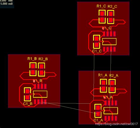
The use of microvias, which are smaller than traditional vias, is a hallmark of HDI technology. These microvias allow for more efficient use of space by enabling connections between layers without occupying significant surface area. However, the placement and size of these microvias must be carefully calculated to avoid issues such as signal loss or impedance mismatches. Additionally, the aspect ratio of these vias should be optimized to maintain structural integrity and reliability.
Signal integrity is another critical consideration in HDI flex PCB design.
As circuits become more compact and operate at higher frequencies, the risk of signal degradation increases. To mitigate this, designers must pay close attention to trace width and spacing, ensuring that they are within the tolerances required for the specific application. Moreover, the use of controlled impedance traces can help maintain signal quality, particularly in high-speed digital applications. This requires precise calculations and often involves collaboration with manufacturers to ensure that the design specifications can be met during production.
Thermal management is also a significant concern in HDI flex PCB design.
The compact nature of these circuits can lead to increased heat generation, which, if not properly managed, can affect performance and longevity. Designers must incorporate effective thermal management strategies, such as the use of thermal vias or heat sinks, to dissipate heat efficiently. Additionally, the choice of materials with good thermal conductivity can aid in managing heat distribution across the PCB.
Furthermore, mechanical considerations cannot be overlooked.
The flexibility of HDI flex PCBs is one of their primary advantages, but it also introduces challenges related to mechanical stress and fatigue. Designers must ensure that the bending radius is within acceptable limits to prevent damage to the circuit. Additionally, the use of strain relief features can help distribute mechanical stress more evenly, enhancing the durability of the PCB.
In conclusion, the design of HDI flex PCBs requires a comprehensive understanding of various factors, including material selection, layout design, signal integrity, thermal management, and mechanical considerations. By carefully addressing these aspects, designers can create robust and efficient circuits that meet the demands of modern electronic applications. As technology continues to advance, the importance of these considerations will only grow, underscoring the need for ongoing innovation and expertise in the field of HDI flex PCB design.
Manufacturing Process Of HDI Flex PCB
The manufacturing process of High-Density Interconnect (HDI) flexible printed circuit boards (PCBs) is a sophisticated and intricate procedure that requires precision and advanced technology. HDI flex PCBs are known for their ability to accommodate complex circuitry in compact spaces, making them ideal for modern electronic devices that demand high performance and miniaturization. To understand the manufacturing process, it is essential to explore the various stages involved, each contributing to the overall functionality and reliability of the final product.
Initially, the process begins with the selection of appropriate materials.
The base material for HDI flex PCBs typically consists of a flexible substrate, such as polyimide, which offers excellent thermal stability and flexibility. This substrate is crucial as it allows the PCB to bend and conform to the desired shape without compromising its electrical integrity. Once the substrate is selected, a thin layer of copper is laminated onto it, serving as the conductive layer for the circuit.
Following the material preparation, the next step involves the creation of the circuit pattern.
This is achieved through a process known as photolithography, where a photosensitive resist is applied to the copper layer. The desired circuit pattern is then transferred onto the resist using ultraviolet light. Subsequently, the exposed areas of the resist are developed, revealing the underlying copper, which is then etched away to form the circuit traces. This precise patterning is crucial for ensuring the high-density interconnections that characterize HDI PCBs.
As the process advances, the focus shifts to the formation of microvias, which are small holes that connect different layers of the PCB.
These microvias are created using laser drilling technology, which offers the precision required for such minute features. The drilled holes are then plated with copper to establish electrical connections between the layers. This step is vital for achieving the compact and efficient design that HDI flex PCBs are known for.
Once the microvias are in place, the next phase involves the application of additional layers, if necessary.
This is done through a process called sequential lamination, where multiple layers of dielectric material and copper are alternately stacked and bonded together. Each layer undergoes the same photolithography and etching process to create the desired circuit pattern. This multilayer construction allows for increased circuit density and functionality, catering to the demands of modern electronic applications.
After the layering process, the HDI flex PCB undergoes surface finishing, which involves the application of a protective coating to prevent oxidation and enhance solderability. Common finishes include immersion gold, immersion silver, and organic solderability preservatives. This step ensures the long-term reliability and performance of the PCB in various environmental conditions.
Finally, the completed HDI flex PCB is subjected to rigorous testing and inspection to verify its electrical and mechanical properties.
This includes continuity testing, impedance testing, and visual inspection to identify any defects or inconsistencies. Only after passing these stringent quality checks is the PCB deemed ready for integration into electronic devices.
In conclusion, the manufacturing process of HDI flex PCBs is a complex and meticulous endeavor that combines advanced materials, precision engineering, and cutting-edge technology. Each stage of the process is critical in ensuring the final product meets the high standards required for modern electronic applications. As technology continues to evolve, the demand for HDI flex PCBs is expected to grow, further driving innovation in their manufacturing processes.
Applications Of HDI Flex PCB In Various Industries
High-Density Interconnect (HDI) flexible printed circuit boards (PCBs) have emerged as a pivotal technology in the electronics industry, offering a multitude of applications across various sectors. These advanced PCBs are characterized by their ability to accommodate a higher density of components on a smaller board, thanks to their fine lines, microvias, and high-performance materials. As industries continue to demand more compact, efficient, and reliable electronic solutions, HDI flex PCBs have become increasingly indispensable.
In the consumer electronics sector, HDI flex PCBs are integral to the development of compact and lightweight devices.
Smartphones, tablets, and wearable technology, such as smartwatches and fitness trackers, benefit significantly from the space-saving attributes of HDI flex PCBs. These devices require intricate circuitry within a limited space, and the flexibility of these PCBs allows for innovative designs that enhance functionality without compromising on size or weight. Moreover, the durability and reliability of HDI flex PCBs ensure that these consumer electronics can withstand the rigors of daily use, including bending and twisting.
Transitioning to the automotive industry, HDI flex PCBs play a crucial role in the advancement of modern vehicles.
As cars become increasingly sophisticated with the integration of advanced driver-assistance systems (ADAS), infotainment systems, and electric vehicle (EV) technologies, the demand for compact and efficient electronic components has surged. HDI flex PCBs are ideal for these applications due to their ability to fit into tight spaces and their capacity to handle complex circuitry. They are used in various automotive applications, including engine control units, navigation systems, and battery management systems, contributing to the overall performance and safety of vehicles.
In the realm of medical devices, HDI flex PCBs are instrumental in the miniaturization and enhancement of medical equipment.
Devices such as pacemakers, hearing aids, and diagnostic imaging equipment rely on the precision and reliability of HDI flex PCBs. The flexibility of these PCBs allows for the creation of devices that can conform to the human body, providing comfort and improved functionality. Additionally, the high-density interconnects enable the integration of more features into medical devices, enhancing their diagnostic and therapeutic capabilities.
The aerospace and defense industries also benefit from the unique properties of HDI flex PCBs.
In these sectors, the demand for lightweight, reliable, and high-performance electronic components is paramount. HDI flex PCBs are used in a variety of applications, including avionics, communication systems, and missile guidance systems. Their ability to withstand extreme conditions, such as high temperatures and vibrations, makes them suitable for use in harsh environments. Furthermore, the compact nature of HDI flex PCBs allows for the reduction of weight in aerospace applications, which is critical for fuel efficiency and payload capacity.
In conclusion, the applications of HDI flex PCBs across various industries underscore their versatility and indispensability in modern technology. As the demand for smaller, more efficient, and reliable electronic solutions continues to grow, HDI flex PCBs will undoubtedly play a pivotal role in shaping the future of electronics. Their ability to meet the stringent requirements of diverse sectors, from consumer electronics to aerospace, highlights their significance as a cornerstone of innovation and technological advancement.