Npi pcb assembly
Understanding the Basics of NPI PCB Assembly
In the realm of electronics manufacturing, New Product Introduction (NPI) is a critical phase that bridges the gap between product design and full-scale production. NPI PCB assembly, in particular, plays a pivotal role in ensuring that a new electronic product is ready for market launch. Understanding the basics of NPI PCB assembly involves delving into the processes and considerations that are essential for a successful transition from prototype to production.
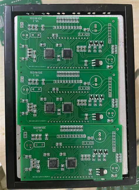
At the heart of NPI PCB assembly is the Printed Circuit Board (PCB), which serves as the foundation for electronic components.
The assembly process begins with the design and layout of the PCB, where engineers meticulously plan the placement of components to optimize functionality and manufacturability. This stage is crucial, as any errors in design can lead to costly revisions later in the process. Therefore, design for manufacturability (DFM) principles are often employed to ensure that the PCB can be efficiently produced without compromising quality.
Once the design is finalized, the next step involves sourcing the necessary components.
This phase requires careful consideration of component availability, lead times, and cost. Selecting the right components is vital, as it impacts not only the performance of the final product but also the overall production timeline. During NPI, manufacturers often work closely with suppliers to secure components that meet the required specifications and are available within the desired timeframe.
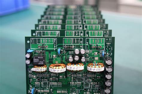
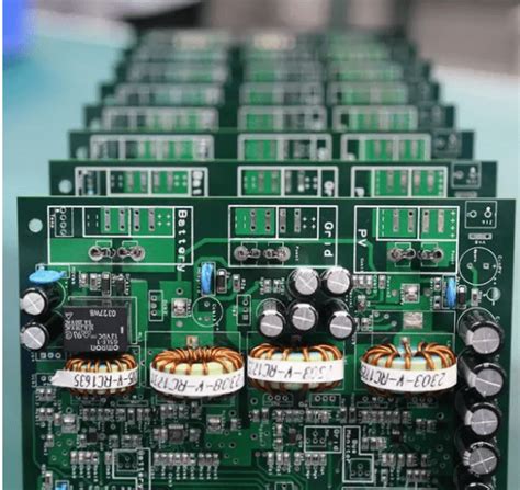
Following component procurement, the focus shifts to the actual assembly of the PCB.
This involves several key processes, including solder paste application, component placement, and soldering. Each of these steps must be executed with precision to ensure that the components are securely attached to the PCB and that electrical connections are reliable. Advanced technologies, such as surface mount technology (SMT) and through-hole technology, are commonly used in this phase to achieve high levels of accuracy and efficiency.
Quality control is an integral part of NPI PCB assembly, as it ensures that the assembled boards meet the required standards and specifications.
Rigorous testing procedures, such as automated optical inspection (AOI) and in-circuit testing (ICT), are employed to detect any defects or inconsistencies. These tests help identify issues early in the process, allowing for timely corrections and minimizing the risk of defects in the final product.
Moreover, NPI PCB assembly is not just about technical execution; it also involves effective project management.
Coordinating the various stages of assembly, from design to testing, requires meticulous planning and communication among all stakeholders. This ensures that the project stays on schedule and within budget, while also allowing for flexibility to address any unforeseen challenges that may arise.
In conclusion, understanding the basics of NPI PCB assembly is essential for anyone involved in the electronics manufacturing industry. It encompasses a range of processes and considerations, from design and component selection to assembly and quality control. By mastering these elements, manufacturers can ensure a smooth transition from prototype to production, ultimately leading to the successful launch of new electronic products. As technology continues to evolve, the importance of efficient and effective NPI PCB assembly will only grow, underscoring its significance in the ever-changing landscape of electronics manufacturing.
Key Challenges in NPI PCB Assembly and How to Overcome Them
In the realm of electronics manufacturing, New Product Introduction (NPI) for Printed Circuit Board (PCB) assembly presents a unique set of challenges that can significantly impact the success of bringing a new product to market. As companies strive to innovate and meet consumer demands, the pressure to efficiently and effectively manage NPI processes becomes paramount.
One of the primary challenges in NPI PCB assembly is the complexity of design verification.
Ensuring that a PCB design is both functional and manufacturable requires meticulous attention to detail. This involves rigorous testing and validation processes to identify potential design flaws early in the development cycle. To overcome this challenge, companies can employ advanced simulation tools and prototyping techniques that allow for iterative testing and refinement, thereby reducing the risk of costly errors during mass production.
Another significant challenge is the coordination between design and manufacturing teams.
Often, there is a disconnect between the two, leading to miscommunications and delays. To address this issue, fostering a collaborative environment where both teams work closely from the outset is crucial. Implementing integrated software solutions that facilitate seamless communication and data sharing can bridge the gap between design and manufacturing, ensuring that both teams are aligned and informed throughout the NPI process.
Supply chain management also poses a considerable challenge in NPI PCB assembly.
The need for timely procurement of components, especially in a global market where supply chain disruptions are not uncommon, can hinder the NPI timeline. To mitigate this risk, companies should establish strong relationships with reliable suppliers and consider diversifying their supplier base to avoid dependency on a single source. Additionally, adopting a proactive approach to inventory management, such as maintaining a buffer stock of critical components, can help cushion the impact of unforeseen supply chain issues.
Moreover, the rapid pace of technological advancements in the electronics industry necessitates continuous adaptation and learning.
Keeping up with the latest technologies and industry standards is essential for successful NPI PCB assembly. Companies must invest in ongoing training and development for their workforce to ensure they possess the necessary skills and knowledge to handle new technologies and processes. This not only enhances the efficiency of the NPI process but also positions the company as a leader in innovation.
Quality assurance is another critical aspect that cannot be overlooked.
Ensuring that the final product meets the highest quality standards is essential for customer satisfaction and brand reputation. Implementing robust quality control measures throughout the NPI process, from design to production, can help identify and rectify issues before they escalate. Utilizing automated inspection systems and adhering to industry standards and certifications can further enhance the quality assurance process.
Finally, cost management is a perennial challenge in NPI PCB assembly.
Balancing the need for high-quality components and processes with budget constraints requires strategic planning and decision-making. Companies can achieve cost efficiency by optimizing design for manufacturability, which involves designing PCBs in a way that simplifies the manufacturing process and reduces material waste. Additionally, leveraging economies of scale and negotiating favorable terms with suppliers can contribute to cost savings.
In conclusion, while NPI PCB assembly presents several challenges, they are not insurmountable. By adopting a proactive and strategic approach, companies can navigate these challenges effectively, ensuring a smooth transition from concept to market-ready product. Through collaboration, innovation, and a commitment to quality, the hurdles of NPI PCB assembly can be transformed into opportunities for growth and success.
The Role of Technology in Streamlining NPI PCB Assembly Processes
In the rapidly evolving landscape of electronics manufacturing, the New Product Introduction (NPI) process for Printed Circuit Board (PCB) assembly plays a pivotal role in bringing innovative products to market efficiently and effectively. As the demand for more complex and compact electronic devices grows, the need for streamlined NPI PCB assembly processes becomes increasingly critical. Technology, in this context, emerges as a key enabler, offering solutions that enhance precision, reduce time-to-market, and improve overall product quality.
To begin with, the integration of advanced design software has revolutionized the initial stages of NPI PCB assembly.
These software tools allow engineers to create detailed and accurate digital prototypes, facilitating early detection of potential design flaws. By simulating various scenarios and stress-testing designs virtually, manufacturers can preemptively address issues that might otherwise lead to costly delays or redesigns. Consequently, this technological advancement not only accelerates the design phase but also ensures a higher degree of reliability in the final product.
Moreover, the advent of automated assembly equipment has significantly transformed the production floor.
Automation technologies, such as robotic pick-and-place machines, have enhanced the precision and speed of component placement on PCBs. These machines are capable of handling thousands of components per hour with remarkable accuracy, thereby minimizing human error and increasing throughput. Additionally, automated optical inspection (AOI) systems have become indispensable in the quality assurance process. By using high-resolution cameras and sophisticated algorithms, AOI systems can quickly identify defects such as misalignments or soldering issues, ensuring that only flawless boards proceed to the next stage of production.
In parallel, the implementation of data analytics and machine learning in NPI PCB assembly processes has opened new avenues for optimization.
By analyzing vast amounts of production data, manufacturers can gain insights into process inefficiencies and areas for improvement. Machine learning algorithms can predict potential failures or bottlenecks, allowing for proactive adjustments that enhance overall efficiency. This data-driven approach not only streamlines operations but also supports continuous improvement initiatives, fostering a culture of innovation and excellence.
Furthermore, the role of the Internet of Things (IoT) in NPI PCB assembly cannot be overstated.
IoT-enabled devices and sensors provide real-time monitoring and control of various assembly parameters, ensuring optimal conditions throughout the production process. This connectivity allows for seamless communication between different stages of assembly, facilitating a more cohesive and integrated workflow. As a result, manufacturers can respond swiftly to any deviations from the norm, maintaining high standards of quality and consistency.
In addition to these technological advancements, the adoption of digital twin technology is gaining traction in the realm of NPI PCB assembly.
By creating a virtual replica of the physical assembly line, manufacturers can simulate and analyze the impact of changes before implementing them in the real world. This capability not only reduces the risk associated with process modifications but also accelerates the decision-making process, enabling faster adaptation to market demands.
In conclusion, the role of technology in streamlining NPI PCB assembly processes is multifaceted and transformative. From design and automation to data analytics and IoT integration, technological innovations are driving significant improvements in efficiency, quality, and speed. As the electronics industry continues to evolve, embracing these advancements will be crucial for manufacturers seeking to maintain a competitive edge and deliver cutting-edge products to consumers worldwide.
Best Practices for Successful NPI PCB Assembly Projects
In the realm of electronics manufacturing, New Product Introduction (NPI) for Printed Circuit Board (PCB) assembly is a critical phase that can determine the success or failure of a product’s market entry. To ensure a seamless transition from design to production, it is essential to adhere to best practices that can mitigate risks and enhance efficiency.
One of the foremost considerations in NPI PCB assembly is thorough design validation.
This involves rigorous testing and simulation to identify potential design flaws before they manifest in the production stage. By employing advanced design software and simulation tools, engineers can predict and rectify issues, thereby reducing the likelihood of costly revisions later in the process.
Following design validation, component selection plays a pivotal role in the success of NPI projects.
Selecting components that are not only suitable for the design but also readily available in the supply chain is crucial. This requires close collaboration with suppliers to ensure that components meet the necessary specifications and are not subject to obsolescence. Additionally, maintaining a flexible approach to component sourcing can help mitigate the impact of supply chain disruptions, which are not uncommon in the electronics industry.
Transitioning from design to production, prototyping serves as an invaluable step in the NPI process.
Prototyping allows for the physical realization of the design, providing an opportunity to test the assembly under real-world conditions. This stage is essential for identifying any unforeseen issues that may not have been apparent during the design phase. By iterating on prototypes, manufacturers can refine the assembly process, ensuring that the final product meets quality standards and performance expectations.
Moreover, effective communication and collaboration among all stakeholders are vital throughout the NPI PCB assembly process.
This includes designers, engineers, suppliers, and manufacturers working in concert to address any challenges that arise. Regular meetings and updates can facilitate the exchange of information and ideas, fostering a collaborative environment that is conducive to problem-solving. By maintaining open lines of communication, potential issues can be identified and resolved promptly, minimizing delays and ensuring that the project remains on schedule.
In addition to collaboration, implementing robust quality control measures is essential for successful NPI PCB assembly.
This involves establishing clear quality standards and conducting thorough inspections at each stage of the assembly process. By employing automated inspection technologies, such as Automated Optical Inspection (AOI) and X-ray inspection, manufacturers can detect defects with high precision, ensuring that only products that meet stringent quality criteria proceed to the next stage.
Finally, a comprehensive review and feedback loop is crucial for continuous improvement in NPI PCB assembly projects.
After the initial production run, gathering feedback from all involved parties can provide valuable insights into areas for improvement. This feedback should be systematically analyzed and used to refine processes, enhance efficiency, and prevent similar issues in future projects. By fostering a culture of continuous improvement, organizations can not only achieve successful NPI PCB assembly but also set the stage for long-term success in the competitive electronics market.
In conclusion, successful NPI PCB assembly projects hinge on a combination of meticulous planning, effective collaboration, and rigorous quality control. By adhering to these best practices, manufacturers can navigate the complexities of the NPI process, ultimately delivering high-quality products that meet market demands and drive business growth.