Machines used for pcb manufacturing
Advancements In PCB Drilling Machines
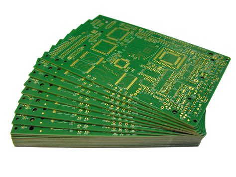
Printed Circuit Boards (PCBs) are the backbone of modern electronic devices, serving as the foundation upon which electronic components are mounted and interconnected. The manufacturing of PCBs involves several intricate processes, among which drilling is a critical step. Drilling is essential for creating vias and through-holes that facilitate electrical connections between different layers of the board. Over the years, advancements in PCB drilling machines have significantly enhanced the efficiency, precision, and capabilities of PCB manufacturing.
Traditionally, mechanical drilling machines were the mainstay in PCB production.
These machines utilized high-speed spindles equipped with drill bits to create holes in the board. While effective, mechanical drilling had limitations in terms of speed and the minimum hole size achievable. As the demand for miniaturization and higher density PCBs grew, the need for more advanced drilling technologies became apparent. This led to the development and adoption of laser drilling machines, which have revolutionized the PCB manufacturing landscape.
Laser drilling machines use focused laser beams to ablate material and create holes with exceptional precision.
One of the primary advantages of laser drilling is its ability to produce extremely small holes, often in the range of micrometers, which is crucial for high-density interconnect (HDI) PCBs. Furthermore, laser drilling is a non-contact process, reducing the risk of mechanical stress and damage to the board. This is particularly beneficial for delicate and thin substrates used in modern electronics.
In addition to precision, laser drilling machines offer remarkable speed, significantly reducing the time required for the drilling process.
This increase in speed is a result of the rapid pulsing capability of lasers, which allows for the quick succession of drilling operations. Consequently, manufacturers can achieve higher throughput, meeting the growing demand for electronic devices without compromising on quality.
Moreover, advancements in laser technology have led to the development of ultraviolet (UV) laser drilling machines.
These machines utilize UV lasers to achieve even greater precision and control, especially when working with complex multilayer PCBs. UV lasers have a shorter wavelength compared to traditional infrared lasers, allowing for finer focus and reduced heat-affected zones. This results in cleaner hole walls and minimal thermal damage to surrounding materials, which is essential for maintaining the integrity of the PCB.
Another significant advancement in PCB drilling machines is the integration of automation and computer numerical control (CNC) systems.
Modern drilling machines are equipped with sophisticated software that allows for precise control over the drilling process. This includes the ability to program complex drilling patterns, adjust parameters in real-time, and monitor the process for quality assurance. Automation not only enhances precision but also reduces the likelihood of human error, leading to more consistent and reliable outcomes.
Furthermore, the incorporation of machine learning and artificial intelligence in PCB drilling machines is an emerging trend that promises to further optimize the manufacturing process. These technologies enable machines to learn from previous operations, adapt to new materials, and predict potential issues before they arise. As a result, manufacturers can achieve higher efficiency, reduce waste, and improve overall product quality.
In conclusion, the advancements in PCB drilling machines have played a pivotal role in meeting the evolving demands of the electronics industry. From the transition from mechanical to laser drilling to the integration of automation and AI, these innovations have enhanced the precision, speed, and capabilities of PCB manufacturing. As technology continues to advance, it is likely that PCB drilling machines will become even more sophisticated, further driving the progress of electronic device production.
The Role Of Pick And Place Machines In PCB Assembly
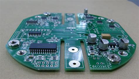
In the intricate world of printed circuit board (PCB) manufacturing, the role of pick and place machines is pivotal. These machines are at the heart of PCB assembly, a process that demands precision, speed, and reliability. As the demand for smaller, more complex electronic devices grows, the importance of efficient PCB assembly becomes increasingly critical. Pick and place machines, therefore, play a crucial role in meeting these demands by automating the placement of components onto the PCB with remarkable accuracy.
To understand the significance of pick and place machines, it is essential to first appreciate the complexity of modern PCBs.
These boards serve as the foundation for electronic devices, providing the necessary pathways for electrical currents to flow between components. As technology advances, PCBs have become more compact and densely populated with components, making manual assembly not only impractical but also prone to errors. This is where pick and place machines come into play, offering a solution that combines speed with precision.
Pick and place machines are designed to handle a wide variety of components, from tiny resistors and capacitors to larger integrated circuits.
They achieve this through a combination of advanced vision systems, precision nozzles, and sophisticated software algorithms. The process begins with the machine identifying the correct component from a reel or tray, using a vacuum nozzle to pick it up. The machine then accurately places the component onto the PCB at the designated location. This entire process is executed with incredible speed, often placing thousands of components per hour.
Moreover, the accuracy of pick and place machines is a testament to their engineering.
These machines are capable of placing components with tolerances as tight as a few micrometers. This level of precision is essential, especially as the size of components continues to shrink. The ability to place components accurately ensures that the electrical connections are reliable, which is crucial for the functionality of the final product.
In addition to speed and precision, pick and place machines offer flexibility.
They can be programmed to handle different types of PCBs and components, making them suitable for both high-volume production and small-batch prototyping. This adaptability is particularly valuable in an industry where product lifecycles are short and customization is often required.
Furthermore, the integration of pick and place machines into the broader PCB manufacturing process enhances overall efficiency.
These machines are typically part of an automated assembly line that includes solder paste application, reflow soldering, and inspection. By automating the component placement step, pick and place machines help reduce the risk of human error, improve throughput, and ensure consistent quality across batches.
As technology continues to evolve, so too do pick and place machines.
Innovations such as machine learning and artificial intelligence are being integrated into these systems, further enhancing their capabilities. These advancements promise to improve the speed and accuracy of component placement even further, while also enabling predictive maintenance and real-time optimization of the assembly process.
In conclusion, pick and place machines are indispensable in the realm of PCB assembly. Their ability to combine speed, precision, and flexibility makes them a cornerstone of modern electronics manufacturing. As the industry continues to push the boundaries of what is possible, these machines will undoubtedly play a key role in shaping the future of electronic devices.
Understanding The Functionality Of Solder Paste Printers
In the intricate world of printed circuit board (PCB) manufacturing, solder paste printers play a pivotal role, serving as the initial step in the assembly process. These machines are designed to apply solder paste onto the PCB, a crucial task that ensures the subsequent placement of components is both accurate and reliable. Understanding the functionality of solder paste printers is essential for appreciating their contribution to the overall efficiency and quality of PCB production.
To begin with, solder paste printers operate by using a stencil to apply solder paste onto the designated pads of a PCB.
The stencil, typically made of stainless steel, contains apertures that correspond to the layout of the PCB. As the printer spreads the solder paste across the stencil, it is deposited onto the board through these apertures. This process requires precision, as the amount and placement of solder paste directly affect the electrical connections and mechanical stability of the final product.
Transitioning to the mechanics of these machines, solder paste printers are equipped with sophisticated control systems that ensure high accuracy and repeatability.
These systems often include vision alignment technology, which uses cameras to align the stencil with the PCB. This alignment is critical, as even minor misalignments can lead to defects such as solder bridges or insufficient solder joints. By employing advanced imaging techniques, solder paste printers can achieve alignment tolerances within micrometers, thereby enhancing the reliability of the soldering process.
Moreover, the consistency of the solder paste application is another vital aspect managed by these machines.
Factors such as the pressure applied during printing, the speed of the squeegee, and the viscosity of the solder paste are meticulously controlled. These parameters must be optimized to accommodate variations in PCB design and environmental conditions. For instance, changes in temperature or humidity can affect the flow characteristics of the solder paste, necessitating adjustments in the printer settings to maintain uniformity.
In addition to their technical capabilities, solder paste printers are integral to the quality control process in PCB manufacturing.
Many modern printers are equipped with inspection systems that verify the accuracy of the solder paste deposition. These systems can detect defects such as insufficient or excessive paste, misalignment, and contamination. By identifying these issues early in the production process, manufacturers can reduce the incidence of defects in the final product, thereby improving yield and reducing costs.
Furthermore, the integration of solder paste printers with other manufacturing equipment is a testament to their importance in the PCB assembly line.
They are often linked with pick-and-place machines and reflow ovens, forming a seamless production flow that enhances efficiency. This integration allows for real-time data exchange and process optimization, ensuring that each stage of the assembly process is synchronized and operating at peak performance.
In conclusion, solder paste printers are indispensable in the realm of PCB manufacturing, providing the foundation for accurate component placement and reliable electrical connections. Their advanced technology and integration capabilities underscore their role in enhancing production efficiency and product quality. As the demand for more complex and miniaturized electronic devices continues to grow, the functionality and precision of solder paste printers will remain a critical factor in meeting the challenges of modern PCB manufacturing.
How Automated Optical Inspection Machines Enhance PCB Quality
In the realm of printed circuit board (PCB) manufacturing, ensuring the highest quality of the final product is paramount. As electronic devices become increasingly complex, the demand for flawless PCBs has surged. This is where Automated Optical Inspection (AOI) machines play a crucial role, significantly enhancing the quality of PCBs. By employing advanced imaging and processing technologies, AOI machines meticulously inspect PCBs for defects, ensuring that only the highest quality boards proceed to the next stages of production.
To begin with, AOI machines utilize high-resolution cameras and sophisticated algorithms to capture detailed images of PCBs
These images are then compared against a predefined set of standards or a “golden board” to identify any discrepancies. This process is not only faster but also more accurate than manual inspection, which is prone to human error. By automating the inspection process, manufacturers can achieve a higher level of consistency and reliability in their products.
Moreover, AOI machines are capable of detecting a wide range of defects, including soldering issues, component misalignments, and surface irregularities.
This comprehensive inspection capability is essential in today’s manufacturing environment, where even the smallest defect can lead to significant performance issues or product failures. By identifying these defects early in the production process, AOI machines help manufacturers address potential problems before they escalate, thereby reducing waste and improving overall efficiency.
In addition to defect detection, AOI machines also contribute to process optimization.
By providing detailed feedback on the types and frequencies of defects, these machines enable manufacturers to pinpoint areas in the production process that require improvement. This data-driven approach allows for continuous process refinement, ultimately leading to higher quality products and reduced production costs. Furthermore, the integration of AOI machines into the manufacturing process facilitates real-time monitoring and control, allowing for immediate corrective actions when necessary.
Another significant advantage of AOI machines is their ability to handle high-volume production with ease.
As the demand for electronic devices continues to grow, manufacturers are under pressure to produce large quantities of PCBs quickly and efficiently. AOI machines are designed to operate at high speeds, inspecting thousands of boards per hour without compromising on accuracy. This capability is essential for meeting tight production schedules and maintaining a competitive edge in the market.
Furthermore, the implementation of AOI machines aligns with the broader trend towards Industry 4.0 and smart manufacturing.
By integrating AOI systems with other automated processes and data analytics tools, manufacturers can create a more interconnected and intelligent production environment. This integration not only enhances quality control but also supports predictive maintenance and supply chain optimization, further boosting operational efficiency.
In conclusion, Automated Optical Inspection machines are indispensable tools in the quest for superior PCB quality. By leveraging advanced imaging technologies and data analytics, these machines provide manufacturers with the means to detect defects early, optimize production processes, and meet the demands of high-volume manufacturing. As the electronics industry continues to evolve, the role of AOI machines in ensuring the quality and reliability of PCBs will only become more critical, underscoring their importance in modern manufacturing.