How to identify multilayer pcb
Understanding The Basics: Key Features Of Multilayer PCBs
Multilayer printed circuit boards (PCBs) are a cornerstone of modern electronic design, offering enhanced functionality and compactness compared to their single-layer counterparts. Understanding the key features of multilayer PCBs is essential for anyone involved in electronics design or manufacturing. These complex structures consist of multiple layers of conductive material, typically copper, separated by insulating layers known as substrates. The primary advantage of multilayer PCBs is their ability to accommodate a higher density of components and interconnections, which is crucial for advanced electronic devices.
One of the most distinguishing features of multilayer PCBs is their layered construction.
Unlike single-layer or double-layer PCBs, which have one or two conductive layers respectively, multilayer PCBs can have three or more layers. These layers are laminated together under high pressure and temperature, creating a single, unified board. This construction allows for more complex circuit designs, as it provides additional surface area for routing traces and placing components. Consequently, multilayer PCBs are often used in applications where space is at a premium, such as in smartphones, laptops, and other compact electronic devices.
Another key feature of multilayer PCBs is their ability to reduce electromagnetic interference (EMI).
The close proximity of the conductive layers allows for better control of the electromagnetic fields generated by the circuit. By strategically placing ground and power planes within the stack-up, designers can create a shielding effect that minimizes EMI. This is particularly important in high-frequency applications, where EMI can significantly impact performance. Furthermore, the use of multiple layers enables the implementation of more sophisticated grounding and power distribution schemes, which can further enhance the board’s performance and reliability.
In addition to EMI reduction, multilayer PCBs offer improved signal integrity.
The additional layers provide more options for routing high-speed signals, allowing designers to optimize trace lengths and minimize signal loss. This is achieved by using controlled impedance traces and differential pairs, which help maintain signal quality over longer distances. As a result, multilayer PCBs are well-suited for applications that require high-speed data transmission, such as telecommunications and networking equipment.
Thermal management is another critical aspect of multilayer PCBs.
The increased density of components and traces can lead to higher heat generation, which must be effectively managed to ensure reliable operation. Multilayer PCBs can incorporate thermal vias and heat sinks to dissipate heat away from critical components. Additionally, the use of specialized materials with high thermal conductivity can further enhance the board’s ability to manage heat. This is particularly important in power electronics and other applications where thermal performance is a key consideration.
Finally, the manufacturing process for multilayer PCBs is more complex than that for single-layer boards.
It involves multiple steps, including layer alignment, lamination, drilling, and plating. Each step must be carefully controlled to ensure the final product meets the required specifications. This complexity can result in higher production costs and longer lead times, but the benefits of multilayer PCBs often outweigh these drawbacks, especially in high-performance applications.
In conclusion, multilayer PCBs are a vital component of modern electronics, offering numerous advantages over simpler board designs. Their layered construction, EMI reduction capabilities, improved signal integrity, and effective thermal management make them ideal for a wide range of applications. Understanding these key features is essential for anyone involved in the design or manufacture of electronic devices, as it enables the creation of more efficient, reliable, and compact products.

Visual Inspection Techniques For Identifying Multilayer PCBs
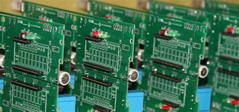
Identifying multilayer printed circuit boards (PCBs) through visual inspection requires a keen eye and a methodical approach. Multilayer PCBs, which consist of multiple layers of conductive material separated by insulating layers, are integral to modern electronic devices due to their ability to support complex circuitry in a compact form. To accurately identify these intricate boards, one must employ a series of visual inspection techniques that reveal the distinct characteristics of multilayer PCBs.
Initially, examining the board’s edge can provide valuable insights.
Multilayer PCBs often display a visible stack of layers when viewed from the side. This stratification is typically more pronounced than in single or double-layer boards, where the layers are fewer and less distinct. By carefully observing the edge, one can often discern the alternating pattern of conductive and insulating layers, which is a hallmark of multilayer construction. This method, however, requires good lighting and sometimes magnification to clearly see the layers, especially in boards with a high layer count.
Furthermore, the presence of vias, which are small holes that allow electrical connections between layers, is another indicator of a multilayer PCB.
These vias can be through-hole, blind, or buried, each serving different purposes in the board’s design. Through-hole vias are visible on both sides of the board, while blind vias connect the outer layer to one or more inner layers without penetrating the entire board. Buried vias, on the other hand, connect internal layers and are not visible from the surface. The density and arrangement of these vias can suggest the complexity and the number of layers within the PCB.
In addition to edge examination and via inspection, the surface complexity of the PCB can also provide clues.
Multilayer PCBs often support more complex and dense circuitry than their single or double-layer counterparts. This complexity is reflected in the intricate network of traces and components on the board’s surface. A densely packed surface with numerous components and interconnections typically indicates a multilayer design, as such complexity necessitates additional layers to accommodate the required circuitry.
Moreover, the board’s thickness can be a subtle yet telling feature.
While not definitive on its own, a thicker board may suggest the presence of multiple layers. However, it is important to consider that board thickness can also be influenced by other factors, such as the type of materials used and the specific application for which the PCB is designed. Therefore, thickness should be evaluated in conjunction with other visual indicators.
Finally, understanding the context in which the PCB is used can aid in identification.
Multilayer PCBs are commonly found in advanced electronic devices such as smartphones, computers, and telecommunications equipment, where space constraints and performance requirements necessitate their use. Recognizing the type of device or application can provide additional context that supports the visual inspection findings.
In conclusion, identifying multilayer PCBs through visual inspection involves a combination of techniques that focus on edge examination, via inspection, surface complexity, and board thickness, all while considering the application context. By employing these methods, one can effectively distinguish multilayer PCBs from simpler designs, thereby gaining a deeper understanding of the board’s construction and potential capabilities.

Differentiating Multilayer PCBs From Single And Double-Layer Boards
In the realm of electronics, printed circuit boards (PCBs) serve as the backbone of most electronic devices, providing the necessary pathways for electrical currents to flow between components.
As technology advances, the complexity and functionality of these boards have increased, leading to the development of multilayer PCBs. Differentiating multilayer PCBs from their single and double-layer counterparts is crucial for engineers and designers who aim to optimize the performance and efficiency of electronic devices.
To begin with, understanding the basic structure of PCBs is essential.
A single-layer PCB, as the name suggests, consists of one layer of conductive material, typically copper, on one side of a non-conductive substrate. This simplicity makes them cost-effective and easy to manufacture, but it also limits their functionality and application. In contrast, double-layer PCBs have conductive material on both sides of the substrate, allowing for more complex circuits and increased component density. However, even double-layer boards can fall short when it comes to meeting the demands of modern electronic devices.
This is where multilayer PCBs come into play.
These boards consist of three or more layers of conductive material, separated by insulating layers, all laminated together into a single, compact structure. The additional layers allow for more intricate circuit designs, greater component density, and improved performance. Identifying a multilayer PCB involves examining several key characteristics that distinguish them from single and double-layer boards.
One of the most apparent differences is the thickness of the board.
Multilayer PCBs are generally thicker due to the multiple layers of conductive and insulating materials. This increased thickness can be observed visually or measured using calipers. Additionally, the presence of vias, which are small holes drilled through the board to connect different layers, is a telltale sign of a multilayer PCB. These vias facilitate electrical connections between layers, enabling complex circuit paths that are not possible with single or double-layer boards.
Another distinguishing feature is the complexity of the circuit design.
Multilayer PCBs often support more sophisticated and densely packed circuits, which can be observed by examining the board’s layout. The intricate network of traces and components is a clear indicator of a multilayer design. Furthermore, the presence of ground and power planes, which are dedicated layers for grounding and power distribution, is a common characteristic of multilayer PCBs. These planes help reduce electromagnetic interference and improve signal integrity, which are critical for high-performance applications.
In addition to these physical attributes, the applications of multilayer PCBs also set them apart.
They are commonly used in advanced electronic devices such as smartphones, computers, and medical equipment, where space is limited, and performance is paramount. The ability to integrate multiple functions into a single board makes multilayer PCBs indispensable in these contexts.
In conclusion, differentiating multilayer PCBs from single and double-layer boards involves examining their structural characteristics, such as thickness, the presence of vias, and circuit complexity. Understanding these differences is vital for selecting the appropriate PCB type for specific applications, ensuring optimal performance and efficiency in electronic devices. As technology continues to evolve, the role of multilayer PCBs in advancing electronic design and functionality will undoubtedly become even more significant.
Advanced Tools And Methods For Multilayer PCB Identification
Identifying multilayer printed circuit boards (PCBs) is a crucial task in the field of electronics, particularly for professionals involved in design, manufacturing, and quality assurance. As technology advances, the complexity of PCBs increases, necessitating advanced tools and methods for accurate identification. Understanding these techniques is essential for ensuring the functionality and reliability of electronic devices.
To begin with, multilayer PCBs are characterized by having more than two layers of conductive material, typically copper, separated by insulating layers.
These layers are laminated together to form a single board. The complexity of these boards allows for more compact and efficient designs, which are essential in modern electronics. However, this complexity also poses challenges in identification and analysis.
One of the primary methods for identifying multilayer PCBs is through visual inspection.
This involves examining the board under a microscope to identify the number of layers and their arrangement. While this method can provide a basic understanding, it is often insufficient for detailed analysis due to the limitations of human vision and the intricate nature of multilayer PCBs. Therefore, more advanced tools are required to gain a comprehensive understanding.
X-ray inspection is a widely used technique that allows for non-destructive analysis of multilayer PCBs.
By using X-rays, technicians can view the internal structure of the board without disassembling it. This method provides a clear image of the layers, vias, and traces, enabling accurate identification of the board’s configuration. X-ray inspection is particularly useful for detecting defects such as misalignments, voids, or shorts that may not be visible through visual inspection alone.
In addition to X-ray inspection, automated optical inspection (AOI) systems are employed to enhance the identification process.
AOI systems use high-resolution cameras and sophisticated algorithms to analyze the surface of the PCB. These systems can quickly identify discrepancies in the board’s design, such as missing components or incorrect placements. While AOI is primarily used for surface inspection, it can also provide valuable information about the board’s overall structure when combined with other methods.
Another advanced method for multilayer PCB identification is the use of computer-aided design (CAD) software.
CAD tools allow engineers to create detailed models of PCBs, including all layers and components. By comparing the physical board with its CAD model, discrepancies can be identified and addressed. This method is particularly useful during the design and prototyping stages, as it ensures that the final product matches the intended design.
Furthermore, electrical testing is an essential tool for identifying multilayer PCBs.
This involves applying electrical signals to the board and measuring the response. By analyzing the electrical characteristics, such as resistance, capacitance, and inductance, technicians can infer the board’s structure and identify any potential issues. Electrical testing is often used in conjunction with other methods to provide a comprehensive analysis.
In conclusion, identifying multilayer PCBs requires a combination of advanced tools and methods. Visual inspection, while useful, is often supplemented by X-ray inspection, automated optical inspection, CAD software, and electrical testing to achieve accurate results. As technology continues to evolve, these methods will become increasingly sophisticated, enabling more precise identification and analysis of multilayer PCBs. Understanding and utilizing these advanced techniques is essential for professionals in the electronics industry to ensure the quality and reliability of their products.