Hdi pcb process flow
Understanding The Basics Of HDI PCB Design
High-Density Interconnect (HDI) printed circuit boards (PCBs) represent a significant advancement in the field of electronics, offering a compact and efficient solution for modern electronic devices.
Understanding the basics of HDI PCB design is crucial for engineers and designers aiming to leverage these benefits in their projects. The HDI PCB process flow involves several intricate steps, each contributing to the overall functionality and reliability of the final product.
Initially, the design phase is paramount, where engineers utilize advanced software tools to create detailed schematics and layouts.
This stage involves defining the board’s dimensions, layer stack-up, and the placement of components. The goal is to maximize the use of available space while ensuring signal integrity and minimizing electromagnetic interference. Transitioning from design to fabrication, the next step involves the preparation of materials. HDI PCBs typically use high-quality substrates like FR-4 or polyimide, chosen for their excellent thermal and electrical properties. These materials are crucial for supporting the fine features and dense routing required in HDI designs.
Following material preparation, the process moves to the drilling stage, which is notably different from traditional PCB manufacturing.
HDI PCBs employ microvias, which are significantly smaller than standard vias, allowing for higher component density and improved electrical performance. Laser drilling technology is often used to create these microvias with precision, ensuring that they meet the stringent tolerances required for HDI applications. As the process continues, the next phase involves the application of conductive layers. This is achieved through a series of plating processes, including electroless copper deposition and electroplating. These steps are critical for forming the electrical pathways that connect various components on the board.
Subsequently, the focus shifts to the imaging and etching processes.
Photolithography is employed to transfer the circuit pattern onto the board, using a photosensitive resist and ultraviolet light. This step is followed by etching, where unwanted copper is removed, leaving behind the desired circuit traces. The precision of these processes is vital, as any deviation can lead to defects that compromise the board’s performance. As the HDI PCB process flow progresses, the next stage involves the application of solder mask and surface finish. The solder mask is a protective layer that prevents solder bridges and protects the board from environmental factors. Various surface finishes, such as ENIG (Electroless Nickel Immersion Gold) or HASL (Hot Air Solder Leveling), are applied to enhance solderability and protect exposed copper areas.
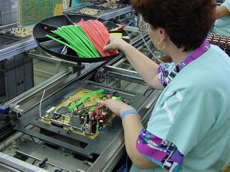
Finally, the assembly phase brings together all the components, using techniques like surface mount technology (SMT) to place and solder components onto the board.
This step requires precision and care, as the high component density of HDI PCBs leaves little room for error. Once assembly is complete, rigorous testing ensures that the board meets all design specifications and functions as intended. In conclusion, the HDI PCB process flow is a complex sequence of steps that demands precision and expertise. Each phase, from design to testing, plays a crucial role in producing a reliable and efficient product. Understanding these basics is essential for anyone involved in the design and manufacture of HDI PCBs, as it lays the foundation for creating cutting-edge electronic devices that meet the demands of today’s technology-driven world.

Step-By-Step Guide To HDI PCB Manufacturing
The process of manufacturing High-Density Interconnect (HDI) printed circuit boards (PCBs) is a sophisticated and intricate procedure that requires precision and attention to detail. HDI PCBs are known for their compact design and high performance, making them essential in modern electronics where space and efficiency are paramount. To understand the HDI PCB manufacturing process, it is crucial to explore each step involved, beginning with the design phase and culminating in the final inspection.
Initially, the process begins with the design and layout of the PCB.
Engineers utilize advanced software tools to create a detailed blueprint of the circuit board, ensuring that all components are optimally placed to achieve the desired functionality. This design phase is critical, as it sets the foundation for the entire manufacturing process. Once the design is finalized, it is converted into a format suitable for production, typically a Gerber file, which contains all the necessary information for the subsequent steps.
Following the design phase, the next step is the preparation of the substrate material.
HDI PCBs often use materials such as FR4, a type of fiberglass-reinforced epoxy laminate, due to its excellent electrical insulation properties and mechanical strength. The substrate is meticulously cleaned to remove any contaminants that could affect the adhesion of subsequent layers. This cleaning process is vital to ensure the integrity and reliability of the final product.
Subsequently, the process moves to the creation of microvias, which are small holes that connect different layers of the PCB.
These microvias are a defining feature of HDI PCBs, allowing for higher component density and improved electrical performance. Laser drilling is commonly employed to create these microvias due to its precision and ability to produce extremely small holes. Once drilled, the microvias are plated with copper to establish electrical connections between the layers.
The next phase involves the application of copper layers through a process known as electroless copper deposition.
This step is crucial for forming the conductive pathways on the PCB. The board is then subjected to a series of photolithography processes, where a photosensitive film is applied, exposed to ultraviolet light through a mask, and developed to reveal the desired circuit pattern. This pattern is subsequently etched to remove excess copper, leaving behind the intricate network of conductive traces.
As the process continues, additional layers may be added to the PCB, each undergoing similar steps of drilling, plating, and patterning.
This multilayer construction is a hallmark of HDI technology, allowing for complex circuits within a compact form factor. Throughout these stages, quality control measures are rigorously applied to ensure that each layer aligns perfectly and that the electrical connections are flawless.
Finally, the HDI PCB undergoes a series of inspections and tests to verify its functionality and reliability
Automated optical inspection (AOI) systems are used to detect any defects in the circuit patterns, while electrical testing ensures that all connections are intact and performing as expected. Once the board passes these stringent quality checks, it is ready for assembly and integration into electronic devices.
In conclusion, the HDI PCB manufacturing process is a meticulous and highly technical endeavor that demands precision at every stage. From the initial design to the final inspection, each step is carefully executed to produce a high-performance circuit board that meets the demands of modern electronic applications. Through this detailed process, HDI PCBs continue to play a crucial role in advancing technology and enabling the development of increasingly sophisticated electronic devices.
Key Challenges In HDI PCB Process Flow
The process flow of High-Density Interconnect (HDI) printed circuit boards (PCBs) is a sophisticated and intricate procedure that presents several key challenges. As the demand for more compact and efficient electronic devices continues to rise, the need for HDI PCBs has become increasingly prevalent.
These PCBs are characterized by their higher wiring density per unit area, which is achieved through the use of finer lines and spaces, smaller vias, and capture pads. However, the complexity of the HDI PCB process flow introduces a range of challenges that manufacturers must navigate to ensure the production of high-quality boards.
One of the primary challenges in the HDI PCB process flow is the precision required in the fabrication of microvias.
Microvias are essential for connecting different layers of the PCB, and their small size necessitates advanced drilling techniques. Laser drilling is commonly employed to achieve the necessary precision, but this method requires careful control to avoid defects such as misalignment or incomplete drilling. Furthermore, the aspect ratio of microvias, which is the ratio of the depth to the diameter, must be meticulously managed to ensure reliable electrical connections. This necessitates a high level of expertise and sophisticated equipment, which can be a significant barrier for manufacturers.
In addition to microvia fabrication, the lamination process in HDI PCB manufacturing poses its own set of challenges.
The lamination process involves bonding multiple layers of the PCB together, and any misalignment during this stage can lead to defects that compromise the board’s functionality. The use of thin dielectric materials in HDI PCBs further complicates this process, as these materials are more susceptible to warping and other forms of distortion. Consequently, manufacturers must implement stringent quality control measures to ensure that each layer is accurately aligned and securely bonded.
Another significant challenge in the HDI PCB process flow is the management of thermal and mechanical stresses.
As electronic devices become more powerful, the heat generated by components increases, which can lead to thermal expansion and contraction of the PCB materials. This thermal cycling can cause mechanical stresses that may result in delamination or cracking of the board. To mitigate these risks, manufacturers must carefully select materials with compatible coefficients of thermal expansion and employ advanced thermal management techniques.
Moreover, the miniaturization of components in HDI PCBs necessitates the use of advanced soldering techniques to ensure reliable connections.
The smaller pads and tighter spacing increase the risk of solder bridging and other defects, which can lead to short circuits or open connections. Therefore, manufacturers must employ precise soldering methods, such as reflow soldering with controlled temperature profiles, to achieve high-quality solder joints.
Finally, the testing and inspection of HDI PCBs present additional challenges due to their complexity and density.
Traditional testing methods may not be sufficient to detect all potential defects, necessitating the use of advanced inspection technologies such as automated optical inspection (AOI) and X-ray inspection. These technologies allow for the detection of hidden defects and ensure that the final product meets the required specifications.
In conclusion, the HDI PCB process flow is fraught with challenges that require careful consideration and advanced techniques to overcome. From microvia fabrication to lamination, thermal management, soldering, and inspection, each stage of the process demands precision and expertise. As technology continues to evolve, manufacturers must remain vigilant and adaptable to meet the growing demands for high-performance HDI PCBs.
Innovations In HDI PCB Technology And Their Impact
High-Density Interconnect (HDI) printed circuit boards (PCBs) have become a cornerstone in the advancement of modern electronics, driven by the relentless pursuit of miniaturization and enhanced performance. As electronic devices continue to shrink in size while demanding greater functionality, the innovations in HDI PCB technology have played a pivotal role in meeting these challenges. The HDI PCB process flow, characterized by its intricate design and manufacturing techniques, has undergone significant transformations, leading to substantial impacts on the electronics industry.
To begin with, the HDI PCB process flow involves several critical stages, each contributing to the overall efficiency and capability of the final product.
Initially, the design phase is crucial, as it sets the foundation for the entire manufacturing process. Advanced computer-aided design (CAD) tools are employed to create complex multilayer designs that accommodate the high-density requirements. These tools allow for precise placement of microvias, blind vias, and buried vias, which are essential for connecting the multiple layers of the PCB. The ability to incorporate these features has been a significant innovation, enabling the reduction of board size while increasing the number of connections.
Following the design phase, the fabrication process begins, which includes the preparation of the substrate material, typically a high-performance laminate.
The choice of material is critical, as it must withstand the thermal and mechanical stresses encountered during operation. Innovations in material science have led to the development of substrates with superior thermal conductivity and electrical insulation properties, enhancing the reliability and performance of HDI PCBs. Moreover, the use of laser drilling technology has revolutionized the creation of microvias, allowing for precise and efficient drilling of extremely small holes, which are essential for high-density interconnections.
As the process continues, the application of conductive layers through techniques such as electroless copper plating ensures robust electrical connections between the various layers.
This step is followed by the application of solder masks and surface finishes, which protect the board and improve its solderability. The advancements in these areas have resulted in improved durability and performance of HDI PCBs, making them suitable for a wide range of applications, from consumer electronics to aerospace and medical devices.
Furthermore, the testing and quality assurance phase is integral to the HDI PCB process flow.
Rigorous testing protocols, including electrical testing and inspection for defects, ensure that the final product meets the stringent standards required for high-performance applications. Innovations in testing methodologies, such as automated optical inspection (AOI) and X-ray inspection, have enhanced the ability to detect and rectify defects early in the production process, thereby reducing waste and improving yield.
In conclusion, the innovations in HDI PCB technology have significantly impacted the electronics industry by enabling the production of smaller, more powerful, and reliable devices. The advancements in design tools, materials, fabrication techniques, and testing methodologies have collectively contributed to the evolution of HDI PCBs. As technology continues to advance, it is anticipated that further innovations will emerge, driving the development of even more sophisticated electronic devices. The ongoing improvements in HDI PCB process flow not only reflect the industry’s response to current demands but also set the stage for future technological breakthroughs.