Hdi pcb construction
Understanding The Basics Of HDI PCB Construction
High-Density Interconnect (HDI) Printed Circuit Boards (PCBs) represent a significant advancement in the field of electronics, offering a compact and efficient solution for modern electronic devices.
Understanding the basics of HDI PCB construction is essential for those involved in electronics design and manufacturing, as these boards are increasingly becoming the standard in the industry.
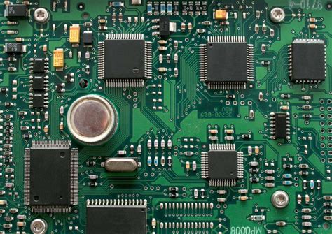
HDI PCBs are characterized by their higher wiring density per unit area compared to traditional PCBs, which is achieved through the use of finer lines and spaces, smaller vias, and capture pads. This increased density allows for more components to be placed on both sides of the board, facilitating the creation of smaller, lighter, and more powerful electronic devices.
The construction of HDI PCBs involves several key processes that distinguish them from conventional PCBs.
One of the primary techniques used in HDI PCB construction is the use of microvias, which are significantly smaller than the vias used in traditional PCBs. Microvias are typically drilled using laser technology, allowing for precise and accurate placement. These microvias enable the interconnection of multiple layers within the PCB, which is crucial for achieving the high-density interconnectivity that HDI boards are known for. Furthermore, the use of microvias reduces the need for through-hole vias, which can take up valuable space on the board and limit design flexibility.
In addition to microvias, HDI PCBs often incorporate blind and buried vias.
Blind vias connect an outer layer to one or more inner layers but do not pass through the entire board, while buried vias connect only internal layers and are not visible from the outside. These types of vias contribute to the efficient use of space within the PCB, allowing for more complex and compact designs. The combination of microvias, blind vias, and buried vias enables designers to create multi-layer boards with intricate routing paths, which is essential for modern electronic devices that require high-speed signal transmission and reduced electromagnetic interference.
Another important aspect of HDI PCB construction is the use of advanced materials and fabrication techniques.
The materials used in HDI PCBs must be able to withstand the higher temperatures and mechanical stresses associated with the increased density and complexity of these boards. As a result, high-performance laminates and substrates are often employed, providing the necessary thermal and mechanical stability. Additionally, the fabrication process for HDI PCBs involves advanced techniques such as sequential lamination and laser direct imaging, which allow for the precise creation of fine lines and spaces required for high-density designs.
The benefits of HDI PCB construction are numerous, making them an attractive option for a wide range of applications.
The increased component density and reduced size of HDI PCBs make them ideal for use in consumer electronics, such as smartphones, tablets, and wearable devices, where space is at a premium. Moreover, the improved electrical performance and reliability of HDI PCBs make them suitable for use in high-performance computing, telecommunications, and automotive applications. As technology continues to advance, the demand for HDI PCBs is expected to grow, driven by the need for smaller, faster, and more efficient electronic devices.
In conclusion, understanding the basics of HDI PCB construction is crucial for those involved in the design and manufacture of modern electronic devices. The use of microvias, advanced materials, and sophisticated fabrication techniques allows for the creation of compact, high-performance PCBs that meet the demands of today’s technology-driven world. As the industry continues to evolve, HDI PCBs will undoubtedly play a pivotal role in shaping the future of electronics.
Key Benefits Of HDI PCB Technology In Modern Electronics
High-Density Interconnect (HDI) Printed Circuit Boards (PCBs) have become a cornerstone in the advancement of modern electronics, offering a multitude of benefits that cater to the ever-evolving demands of technology. As electronic devices continue to shrink in size while increasing in functionality, the role of HDI PCB technology becomes increasingly pivotal.
One of the primary advantages of HDI PCBs is their ability to support miniaturization.
By utilizing finer lines and spaces, smaller vias, and higher connection pad density, HDI technology allows for the design of more compact and lightweight devices. This is particularly beneficial in the production of smartphones, tablets, and wearable technology, where space is at a premium and every millimeter counts.
In addition to enabling smaller device footprints, HDI PCBs also enhance electrical performance.
The reduced distance between components and the use of microvias contribute to lower signal loss and improved signal integrity. This is crucial in high-speed applications where maintaining signal quality is essential for optimal performance. Furthermore, the ability to incorporate multiple layers in HDI PCBs allows for more complex routing, which can accommodate the intricate designs required by modern electronic devices. This complexity does not come at the cost of reliability; in fact, HDI PCBs are known for their robustness and durability, making them suitable for use in demanding environments.
Another significant benefit of HDI PCB technology is its contribution to increased functionality.
By allowing for more components to be placed on a single board, HDI PCBs enable the integration of additional features and capabilities within a device. This is particularly advantageous in the development of multifunctional gadgets that require a high level of integration without compromising on performance. Moreover, the use of advanced materials and manufacturing techniques in HDI PCB construction can lead to improved thermal management. This is essential in preventing overheating and ensuring the longevity of electronic components, especially in high-power applications.
The economic advantages of HDI PCBs should not be overlooked. While the initial cost of HDI PCB production may be higher than that of traditional PCBs, the long-term benefits often outweigh these costs.
The ability to reduce the number of layers and components needed can lead to cost savings in materials and assembly. Additionally, the enhanced performance and reliability of HDI PCBs can result in lower maintenance and repair costs over the lifespan of the device. This makes HDI technology an attractive option for manufacturers looking to optimize both performance and cost-efficiency.
In conclusion, the key benefits of HDI PCB technology in modern electronics are manifold. From enabling miniaturization and enhancing electrical performance to increasing functionality and offering economic advantages, HDI PCBs are integral to the development of cutting-edge electronic devices. As technology continues to advance, the demand for more sophisticated and efficient solutions will only grow, further solidifying the importance of HDI PCB technology in the electronics industry. By embracing these advancements, manufacturers can continue to push the boundaries of what is possible, delivering innovative products that meet the needs of an increasingly connected world.
Challenges And Solutions In HDI PCB Manufacturing
High-Density Interconnect (HDI) printed circuit boards (PCBs) have become a cornerstone in the advancement of modern electronics, offering enhanced performance and miniaturization capabilities. However, the manufacturing of HDI PCBs presents a unique set of challenges that require innovative solutions to ensure reliability and efficiency.
One of the primary challenges in HDI PCB manufacturing is the precise alignment and registration of multiple layers.
As HDI PCBs often involve complex multilayer designs with microvias, any misalignment can lead to circuit failures or reduced performance. To address this, manufacturers employ advanced laser drilling techniques and automated optical inspection systems. These technologies ensure that each layer is accurately aligned, thereby minimizing the risk of defects.
Another significant challenge is the management of thermal and mechanical stresses.
HDI PCBs are typically used in high-performance applications where heat dissipation is critical. The dense circuitry and compact design can exacerbate thermal issues, leading to potential overheating and failure. To mitigate this, manufacturers utilize materials with high thermal conductivity and incorporate thermal vias to enhance heat dissipation. Additionally, the use of advanced simulation tools allows engineers to predict and address potential thermal issues during the design phase, ensuring that the final product can withstand the operational demands.
The miniaturization of components in HDI PCBs also poses challenges in terms of signal integrity and electromagnetic interference (EMI).
As traces become narrower and components are placed closer together, the risk of signal degradation and crosstalk increases. To combat these issues, manufacturers employ techniques such as controlled impedance routing and the use of ground planes to maintain signal integrity. Furthermore, advanced shielding materials and design strategies are implemented to minimize EMI, ensuring that the HDI PCBs perform optimally in their intended applications.
Material selection is another critical aspect of HDI PCB manufacturing that presents its own set of challenges.
The materials used must not only support the electrical and thermal requirements but also be compatible with the manufacturing processes. For instance, the choice of substrate material can significantly impact the board’s performance and reliability. Manufacturers often opt for high-performance laminates that offer low dielectric constants and high thermal stability. However, these materials can be more expensive and challenging to work with, necessitating careful consideration and optimization of the manufacturing process.
In addition to these technical challenges, HDI PCB manufacturing also faces economic and logistical hurdles.
The complexity of the manufacturing process can lead to higher production costs and longer lead times. To address these issues, manufacturers are increasingly adopting automation and lean manufacturing principles to streamline production and reduce costs. By optimizing workflows and employing advanced manufacturing technologies, companies can improve efficiency and maintain competitiveness in the market.
In conclusion, while HDI PCB manufacturing presents a range of challenges, the industry has developed a variety of solutions to overcome these obstacles. Through the use of advanced technologies, careful material selection, and strategic design practices, manufacturers can produce high-quality HDI PCBs that meet the demands of modern electronic applications. As technology continues to evolve, ongoing research and development will be essential in addressing emerging challenges and further enhancing the capabilities of HDI PCBs.
Innovations And Future Trends In HDI PCB Design
High-Density Interconnect (HDI) printed circuit boards (PCBs) have become a cornerstone in the advancement of modern electronics, driven by the relentless pursuit of miniaturization and enhanced performance. As electronic devices continue to shrink in size while demanding greater functionality, HDI PCBs offer a solution by enabling more complex circuitry within a smaller footprint. This innovation is achieved through the use of finer lines and spaces, smaller vias, and higher connection pad density, which collectively contribute to the enhanced capabilities of HDI PCBs.
One of the key innovations in HDI PCB design is the use of microvias, which are significantly smaller than traditional vias.
These microvias allow for more interconnections in a given area, facilitating the design of multi-layered boards that are essential for modern electronic devices. The ability to stack multiple layers of circuitry not only increases the functionality of the device but also improves signal integrity and reduces electromagnetic interference. As a result, HDI PCBs are particularly advantageous in applications where space is at a premium, such as in smartphones, tablets, and wearable technology.
Moreover, the materials used in HDI PCB construction have also seen significant advancements.
High-performance laminates and substrates are now employed to withstand the increased thermal and mechanical stresses associated with high-density designs. These materials offer improved thermal management, which is crucial for maintaining the reliability and longevity of electronic components. Additionally, the use of advanced soldering techniques and surface finishes ensures robust connections and enhances the overall durability of the PCB.
As we look to the future, several trends are poised to shape the evolution of HDI PCB design.
One such trend is the integration of flexible and rigid-flex PCBs, which combine the benefits of both rigid and flexible circuits. This hybrid approach allows for greater design versatility, enabling the creation of complex shapes and configurations that can conform to the contours of the device. This is particularly beneficial in the development of compact and lightweight electronics, where traditional rigid PCBs may be too bulky or restrictive.
Another emerging trend is the incorporation of advanced manufacturing techniques, such as laser direct imaging (LDI) and additive manufacturing.
These technologies offer greater precision and efficiency in the production of HDI PCBs, allowing for even finer features and more intricate designs. As these manufacturing processes continue to evolve, they are expected to further push the boundaries of what is possible in HDI PCB construction.
Furthermore, the rise of the Internet of Things (IoT) and the proliferation of connected devices are driving the demand for HDI PCBs with enhanced connectivity and functionality.
As devices become more interconnected, the need for PCBs that can support high-speed data transmission and complex communication protocols becomes increasingly critical. HDI PCBs, with their ability to accommodate high-density interconnections and advanced signal processing capabilities, are well-suited to meet these demands.
In conclusion, the innovations and future trends in HDI PCB design are set to revolutionize the electronics industry. With advancements in materials, manufacturing techniques, and design approaches, HDI PCBs are poised to enable the next generation of electronic devices. As technology continues to evolve, the role of HDI PCBs in facilitating more compact, efficient, and powerful electronics will undoubtedly become even more significant.