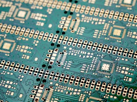
Ceramic pcb substrate
Advantages Of Ceramic PCB Substrate In High-Frequency Applications
Ceramic PCB substrates have emerged as a pivotal component in the realm of high-frequency applications, offering a multitude of advantages that make them an ideal choice for engineers and designers. As the demand for high-performance electronic devices continues to escalate, the need for substrates that can withstand rigorous conditions while maintaining optimal functionality becomes increasingly critical. Ceramic substrates, with their unique properties, address these demands effectively, providing a robust platform for high-frequency circuits.
One of the foremost advantages of ceramic PCB substrates is their excellent thermal conductivity.
In high-frequency applications, managing heat dissipation is crucial to ensure the reliability and longevity of electronic components. Ceramic materials, such as aluminum oxide (Al2O3) and aluminum nitride (AlN), exhibit superior thermal conductivity compared to traditional FR-4 substrates. This property allows for efficient heat transfer away from heat-generating components, thereby reducing the risk of thermal-related failures and enhancing the overall performance of the device.
In addition to thermal management, ceramic substrates offer exceptional electrical insulation properties.
This is particularly important in high-frequency applications where signal integrity is paramount. The low dielectric constant and loss tangent of ceramic materials minimize signal distortion and attenuation, ensuring that high-frequency signals are transmitted with minimal loss. Consequently, this leads to improved signal quality and performance, which is essential for applications such as RF communication systems, microwave circuits, and radar technologies.
Moreover, ceramic substrates are renowned for their mechanical strength and durability.
Unlike their polymer-based counterparts, ceramic materials are inherently resistant to environmental factors such as moisture, chemicals, and temperature fluctuations. This resilience makes them suitable for use in harsh environments where reliability is non-negotiable. Furthermore, the rigidity of ceramic substrates provides a stable platform for mounting components, reducing the risk of mechanical failure due to vibrations or physical stress.
Another significant advantage of ceramic PCB substrates is their compatibility with advanced manufacturing processes.
The ability to fabricate fine features and complex geometries on ceramic substrates allows for the integration of miniaturized components and high-density interconnects. This is particularly beneficial in high-frequency applications where space constraints and the need for compact designs are prevalent. Additionally, ceramic substrates can be easily metallized, enabling the creation of reliable electrical connections and facilitating the integration of various components.
Transitioning to the aspect of cost-effectiveness, it is worth noting that while ceramic substrates may have a higher initial cost compared t3o traditional materials, their long-term benefits often outweigh the upfront investment.
The enhanced performance, reliability, and longevity of devices utilizing ceramic substrates can lead to reduced maintenance costs and fewer replacements over time. This makes them a cost-effective solution for high-frequency applications where performance and reliability are critical.
In conclusion, the advantages of ceramic PCB substrates in high-frequency applications are manifold. Their superior thermal conductivity, excellent electrical insulation, mechanical strength, and compatibility with advanced manufacturing processes make them an indispensable choice for engineers seeking to optimize the performance of high-frequency circuits. As technology continues to advance and the demand for high-performance electronic devices grows, ceramic substrates are poised to play an increasingly vital role in meeting the challenges of high-frequency applications.
Thermal Management Solutions Using Ceramic PCB Substrates
In the realm of electronic design and manufacturing, thermal management is a critical consideration, particularly as devices become more compact and powerful. One innovative solution that has gained prominence is the use of ceramic PCB substrates. These substrates offer a range of benefits that make them particularly well-suited for applications where efficient heat dissipation is paramount. As electronic components generate heat during operation, managing this thermal output is essential to ensure reliability and longevity. Ceramic PCB substrates, with their superior thermal conductivity, provide an effective means of addressing these challenges.
Ceramic materials, such as aluminum oxide (Al2O3), aluminum nitride (AlN), and beryllium oxide (BeO), are commonly used in the fabrication of these substrates
Each of these materials possesses unique properties that contribute to their effectiveness in thermal management. For instance, aluminum nitride is renowned for its high thermal conductivity, which is significantly greater than that of traditional FR-4 substrates. This property allows for rapid heat dissipation away from critical components, thereby reducing the risk of overheating and subsequent failure.
Moreover, ceramic substrates exhibit excellent thermal stability, which is crucial in environments subject to fluctuating temperatures.
Unlike organic substrates, ceramics maintain their structural integrity and performance characteristics over a wide temperature range. This stability ensures that electronic devices can operate reliably even under extreme conditions, making ceramic PCB substrates an ideal choice for aerospace, automotive, and industrial applications where temperature variations are common.
In addition to their thermal properties, ceramic substrates offer electrical insulation capabilities that are essential for maintaining the performance of electronic c
ircuits. The inherent dielectric strength of ceramics prevents electrical leakage and ensures signal integrity, which is vital for high-frequency applications. This combination of thermal and electrical properties makes ceramic substrates a versatile solution for a variety of electronic applications.
Furthermore, the mechanical robustness of ceramic materials contributes to the durability of the substrates. They are resistant to wear and corrosion, which enhances the longevity of the electronic devices in which they are used. This durability is particularly beneficial in harsh environments where exposure to chemicals or mechanical stress is a concern. As a result, ceramic PCB substrates are increasingly being adopted in sectors where reliability and performance are non-negotiable.
Despite these advantages, it is important to acknowledge the challenges associated with ceramic PCB substrates.
The manufacturing process can be more complex and costly compared to traditional substrates, which may impact the overall cost of the final product. However, the long-term benefits of improved thermal management and device reliability often outweigh these initial costs, especially in high-performance applications.
In conclusion, ceramic PCB substrates represent a significant advancement in thermal management solutions for electronic devices. Their superior thermal conductivity, electrical insulation, and mechanical durability make them an attractive option for industries that demand high performance and reliability. As technology continues to evolve, the role of ceramic substrates in enhancing the efficiency and longevity of electronic devices is likely to expand, offering new opportunities for innovation in thermal management solutions.
Innovations In Ceramic PCB Substrate Manufacturing Techniques
Ceramic PCB substrates have emerged as a pivotal component in the electronics industry, offering a range of benefits that make them indispensable in various high-performance applications. As the demand for more efficient and reliable electronic devices continues to grow, innovations in ceramic PCB substrate manufacturing techniques have become increasingly important. These advancements not only enhance the performance of electronic devices but also contribute to the miniaturization and durability of components, which are critical in sectors such as telecommunications, automotive, and aerospace.
One of the most significant innovations in ceramic PCB substrate manufacturing is the development of advanced materials that improve thermal conductivity and electrical insulation.
Traditional materials, such as alumina, have been widely used due to their cost-effectiveness and satisfactory performance. However, the introduction of materials like aluminum nitride and silicon nitride has revolutionized the industry. These materials offer superior thermal management capabilities, which are essential for high-power applications where heat dissipation is a critical concern. By effectively managing heat, these advanced materials help prevent overheating, thereby extending the lifespan of electronic components.
In addition to material advancements, the manufacturing processes themselves have seen remarkable improvements.
Techniques such as low-temperature co-fired ceramics (LTCC) and high-temperature co-fired ceramics (HTCC) have been refined to produce substrates with enhanced mechanical strength and precision. LTCC, in particular, allows for the integration of multiple layers of ceramic and metal, enabling the creation of complex circuits with high-density interconnections. This multilayer capability is crucial for modern electronic devices that require compact and efficient designs. Moreover, these processes have been optimized to reduce production costs and increase scalability, making ceramic PCB substrates more accessible to a broader range of applications.
Furthermore, the advent of additive manufacturing, commonly known as 3D printing, has opened new avenues for ceramic PCB substrate production.
This innovative approach allows for the creation of intricate designs that were previously impossible with traditional manufacturing methods. By using 3D printing, manufacturers can produce substrates with customized geometries and embedded components, leading to more efficient and tailored solutions for specific applications. This flexibility not only enhances the performance of electronic devices but also accelerates the prototyping and development phases, enabling faster time-to-market for new products.
Another noteworthy advancement is the improvement in surface finish techniques, which play a crucial role in the performance and reliability of ceramic PCB substrates.
Enhanced surface finish methods, such as laser machining and precision grinding, ensure that the substrates have a smooth and defect-free surface. This is particularly important for applications that require high-frequency signal transmission, as surface imperfections can lead to signal loss and interference. By achieving a superior surface finish, manufacturers can ensure optimal electrical performance and reliability, which are essential for critical applications in industries like aerospace and defense.
In conclusion, the innovations in ceramic PCB substrate manufacturing techniques have significantly contributed to the advancement of electronic devices. Through the development of advanced materials, refined manufacturing processes, the integration of additive manufacturing, and improved surface finish techniques, ceramic PCB substrates have become more efficient, reliable, and versatile. As technology continues to evolve, these innovations will undoubtedly play a crucial role in meeting the ever-increasing demands of the electronics industry, paving the way for more sophisticated and high-performance applications.

Comparing Ceramic PCB Substrates With Traditional FR4 Materials
In the realm of printed circuit boards (PCBs), the choice of substrate material plays a pivotal role in determining the performance, reliability, and longevity of electronic devices. Among the various materials available, ceramic substrates and traditional FR4 materials are two prominent options, each with distinct characteristics and advantages. Understanding the differences between these materials is crucial for engineers and designers aiming to optimize their electronic applications.
Ceramic PCB substrates, typically made from materials such as alumina, aluminum nitride, or beryllium oxide, are renowned for their exceptional thermal conductivity and electrical insulation properties.
These attributes make ceramic substrates particularly suitable for high-power and high-frequency applications where efficient heat dissipation is paramount. In contrast, FR4, a composite material made from woven fiberglass cloth with an epoxy resin binder, is the most commonly used substrate in the PCB industry due to its cost-effectiveness and versatility. However, FR4’s thermal conductivity is significantly lower than that of ceramic substrates, which can be a limiting factor in applications requiring superior thermal management.
Moreover, ceramic substrates exhibit excellent dimensional stability and mechanical strength, which are critical in environments subject to extreme temperatures and mechanical stress.
This stability ensures that the electronic components mounted on ceramic PCBs maintain their integrity and performance over time. On the other hand, FR4 materials, while offering adequate mechanical properties for many applications, may not withstand the same level of thermal and mechanical stress as ceramics. This limitation can lead to potential issues such as warping or delamination under harsh conditions.
In addition to thermal and mechanical considerations, the electrical performance of ceramic substrates is another area where they often surpass FR4 materials.
Ceramics possess a lower dielectric constant and loss tangent, which translates to reduced signal loss and improved high-frequency performance. This characteristic is particularly advantageous in RF and microwave applications, where maintaining signal integrity is crucial. Conversely, while FR4 materials are suitable for a wide range of frequencies, they may not provide the same level of performance in high-frequency scenarios as ceramic substrates.
Despite these advantages, the choice between ceramic and FR4 substrates is not solely based on performance metrics.
Cost is a significant factor influencing the decision-making process. Ceramic substrates are generally more expensive than FR4 materials, both in terms of raw material costs and manufacturing processes. This cost difference can be a deterrent for applications where budget constraints are a primary concern. Consequently, FR4 remains the preferred choice for many consumer electronics and general-purpose applications where the performance benefits of ceramics are not essential.
Furthermore, the manufacturing processes for ceramic and FR4 PCBs differ considerably.
Ceramic PCBs often require specialized techniques such as thick-film or thin-film deposition, which can be more complex and time-consuming than the standard processes used for FR4 boards. This complexity can impact production timelines and scalability, factors that must be weighed against the performance benefits offered by ceramic substrates.
In conclusion, the decision to use ceramic PCB substrates over traditional FR4 materials hinges on a careful evaluation of the specific requirements of the application. While ceramic substrates offer superior thermal, mechanical, and electrical properties, their higher cost and manufacturing complexity may not be justified in all scenarios. Ultimately, the choice between these materials should be guided by a comprehensive assessment of performance needs, budgetary constraints, and production considerations, ensuring that the selected substrate aligns with the overall objectives of the electronic design.