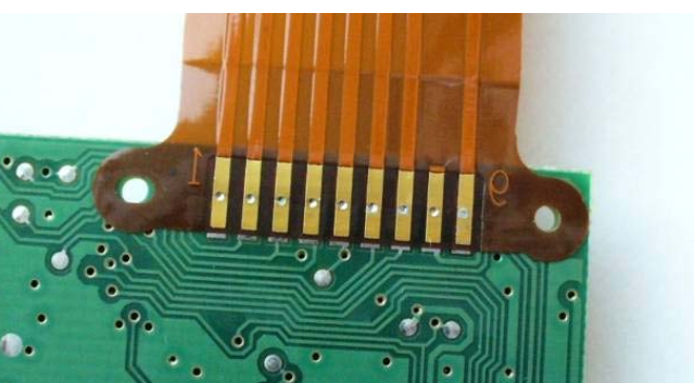
Cutting flex pcb
Advantages Of Using Flex PCBs In Modern Electronics
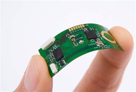
Flexible printed circuit boards (flex PCBs) have become an integral component in the design and manufacturing of modern electronic devices. Their unique properties and advantages over traditional rigid PCBs have made them a preferred choice for engineers and designers seeking to innovate and optimize electronic products.
One of the primary advantages of flex PCBs is their ability to conform to complex shapes and fit into compact spaces, which is increasingly important as electronic devices become smaller and more intricate. This flexibility allows for more creative and efficient use of space within a device, enabling the development of sleeker and more ergonomic products.
In addition to their adaptability, flex PCBs offer significant weight reduction compared to their rigid counterparts.
This is particularly beneficial in applications where weight is a critical factor, such as in aerospace, automotive, and portable consumer electronics. By reducing the overall weight of a device, flex PCBs contribute to improved performance, energy efficiency, and user experience. Moreover, the lightweight nature of flex PCBs does not compromise their durability. On the contrary, they are often more resilient to vibrations and mechanical stress, which enhances the reliability and longevity of the devices in which they are used.
Another notable advantage of flex PCBs is their ability to reduce the number of interconnects required in a circuit.
Traditional rigid PCBs often necessitate multiple connectors and cables to link different components, which can increase the complexity and potential points of failure in a system. Flex PCBs, however, can integrate multiple layers and components into a single, continuous circuit, minimizing the need for additional connectors. This not only simplifies the assembly process but also enhances the overall reliability of the electronic device by reducing the likelihood of connection failures.
Furthermore, flex PCBs offer improved thermal management capabilities.
Their design allows for better heat dissipation, which is crucial in high-performance applications where excessive heat can lead to component failure or reduced efficiency. The ability to manage heat effectively ensures that devices operate within safe temperature ranges, thereby extending their operational life and maintaining optimal performance. This is particularly advantageous in industries such as telecommunications and computing, where devices are often subjected to high thermal loads.
The versatility of flex PCBs also extends to their compatibility with a wide range of materials and technologies.
They can be manufactured using various substrates and conductive materials, allowing for customization to meet specific application requirements. This adaptability makes them suitable for a diverse array of industries, from medical devices to consumer electronics, where different performance characteristics may be needed.
In conclusion, the advantages of using flex PCBs in modern electronics are manifold.
Their flexibility, lightweight nature, durability, and ability to simplify circuit design make them an attractive option for engineers and designers. Additionally, their superior thermal management and compatibility with various materials further enhance their appeal across multiple industries. As technology continues to advance and the demand for more compact, efficient, and reliable electronic devices grows, the role of flex PCBs is likely to become even more prominent, driving innovation and shaping the future of electronics.
Key Considerations For Designing And Cutting Flex PCBs
When designing and cutting flexible printed circuit boards (flex PCBs), several key considerations must be taken into account to ensure optimal performance and reliability. Flex PCBs, known for their ability to bend and conform to various shapes, are increasingly used in modern electronics due to their versatility and space-saving characteristics. However, their unique properties also present distinct challenges that require careful attention during the design and manufacturing processes.
To begin with, material selection is a critical factor in the design of flex PCBs.
The choice of substrate material, typically polyimide, must balance flexibility with durability. Polyimide is favored for its excellent thermal stability and mechanical properties, which are essential for applications that involve dynamic flexing or exposure to harsh environments. Additionally, the copper layer used for the conductive traces must be thin enough to allow for flexibility while maintaining sufficient conductivity. This balance is crucial to prevent cracking or delamination during repeated bending.
Transitioning from material considerations, the design layout of flex PCBs demands meticulous planning.
Unlike rigid PCBs, flex circuits require special attention to trace routing and component placement. Designers must account for the bending areas, ensuring that traces are oriented perpendicular to the bend lines to minimize stress. Furthermore, the use of curved traces instead of sharp angles can help distribute mechanical stress more evenly, reducing the risk of trace breakage. It is also advisable to avoid placing components or vias in areas that will experience significant bending, as this can lead to mechanical failure.
In addition to layout considerations, the cutting process of flex PCBs is another critical aspect that influences the final product’s quality.
Traditional mechanical cutting methods, such as die cutting or routing, can introduce stress points and potential damage to the delicate flex material. Therefore, laser cutting has emerged as a preferred method due to its precision and non-contact nature. Laser cutting allows for intricate shapes and fine details without exerting physical pressure on the material, thereby preserving the integrity of the flex PCB.
Moreover, the choice of cutting method can impact the production efficiency and cost-effectiveness of flex PCBs.
While laser cutting offers superior precision, it may involve higher initial setup costs compared to mechanical methods. However, the reduction in material waste and the ability to produce complex designs can offset these costs in high-volume production scenarios. Therefore, manufacturers must weigh the benefits and drawbacks of each cutting technique in relation to their specific production requirements.
As we consider the broader implications of these design and cutting considerations, it becomes evident that collaboration between designers and manufacturers is essential.
Early communication can help identify potential challenges and optimize the design for manufacturability, ultimately leading to a more efficient production process and a higher-quality end product. By understanding the unique properties of flex PCBs and the intricacies involved in their design and cutting, stakeholders can make informed decisions that enhance the performance and reliability of these versatile electronic components.
In conclusion, the design and cutting of flex PCBs require a comprehensive approach that addresses material selection, layout planning, and cutting techniques. By carefully considering these factors, designers and manufacturers can overcome the challenges associated with flex PCBs and fully leverage their advantages in modern electronic applications. As technology continues to evolve, the demand for flexible and adaptable electronic solutions will only increase, underscoring the importance of mastering these key considerations.

Innovations In Flex PCB Cutting Technology
In recent years, the field of flexible printed circuit boards (flex PCBs) has witnessed significant advancements, particularly in the realm of cutting technology. As the demand for smaller, more efficient electronic devices continues to rise, the need for precise and reliable flex PCB cutting methods has become increasingly critical. This evolution in cutting technology is driven by the necessity to meet the stringent requirements of modern electronics, which demand not only high performance but also cost-effectiveness and environmental sustainability.
One of the most notable innovations in flex PCB cutting technology is the advent of laser cutting.
Laser cutting offers unparalleled precision, allowing for intricate designs and complex geometries that were previously unattainable with traditional mechanical methods. The use of lasers enables manufacturers to achieve clean, burr-free edges, which are essential for maintaining the integrity and functionality of the circuit. Moreover, laser cutting is a non-contact process, which minimizes the risk of damaging the delicate materials used in flex PCBs. This is particularly advantageous when working with thin substrates that are prone to deformation under mechanical stress.
In addition to laser cutting, advancements in automated cutting systems have also played a pivotal role in enhancing the efficiency and accuracy of flex PCB production.
These systems integrate sophisticated software and hardware solutions to optimize the cutting process, reducing waste and improving throughput. By leveraging computer-aided design (CAD) and computer-aided manufacturing (CAM) technologies, automated systems can precisely control the cutting path, ensuring consistent quality across large production runs. This level of automation not only reduces the likelihood of human error but also allows for greater flexibility in design modifications, enabling manufacturers to quickly adapt to changing market demands.
Furthermore, the development of hybrid cutting technologies has opened new possibilities for flex PCB manufacturing.
By combining the strengths of different cutting methods, such as laser and mechanical cutting, hybrid systems can offer a balanced approach that maximizes both speed and precision. For instance, while laser cutting excels in achieving fine details, mechanical cutting can be more efficient for larger, less intricate sections. By strategically employing both techniques, manufacturers can optimize their production processes, resulting in cost savings and improved product quality.
Another significant trend in flex PCB cutting technology is the focus on sustainability.
As environmental concerns continue to shape the electronics industry, manufacturers are increasingly seeking eco-friendly solutions that minimize waste and energy consumption. Innovations such as laser ablation, which uses laser energy to remove material without generating harmful byproducts, are gaining traction as a sustainable alternative to traditional cutting methods. Additionally, the use of recyclable materials and the implementation of closed-loop systems for waste management are becoming standard practices in the industry.
In conclusion, the innovations in flex PCB cutting technology are transforming the landscape of electronic manufacturing.
With the integration of laser cutting, automated systems, hybrid technologies, and sustainable practices, manufacturers are better equipped to meet the demands of modern electronics. These advancements not only enhance the precision and efficiency of flex PCB production but also contribute to a more sustainable and adaptable industry. As technology continues to evolve, it is likely that further innovations will emerge, driving the development of even more sophisticated and environmentally conscious cutting solutions.
Common Challenges And Solutions In Flex PCB Manufacturing
In the realm of modern electronics, flexible printed circuit boards (flex PCBs) have emerged as a pivotal component, offering unparalleled versatility and adaptability. However, the manufacturing of flex PCBs is not without its challenges. Understanding these challenges and their corresponding solutions is crucial for ensuring the reliability and efficiency of the final product.
One of the primary challenges in flex PCB manufacturing is the precise cutting of the flexible substrate.
Unlike rigid PCBs, flex PCBs are made from materials such as polyimide, which are inherently more delicate and prone to damage during the cutting process. This fragility necessitates the use of specialized cutting techniques to prevent tearing or deformation. Laser cutting has become a preferred method due to its precision and ability to produce clean edges without physical contact. However, laser cutting can introduce thermal stress, potentially affecting the material’s properties. To mitigate this, manufacturers often employ controlled laser parameters and cooling techniques to maintain the integrity of the substrate.
Another significant challenge is maintaining dimensional stability throughout the manufacturing process.
Flex PCBs are susceptible to expansion and contraction due to temperature fluctuations and mechanical stress. This can lead to misalignment of circuit traces and components, ultimately affecting the board’s performance. To address this, manufacturers utilize advanced design software that compensates for potential dimensional changes. Additionally, incorporating fiducial markers during the design phase can aid in aligning layers accurately during assembly.
The adhesion of copper traces to the flexible substrate is another critical concern.
Poor adhesion can result in delamination, where the copper separates from the substrate, leading to circuit failure. To enhance adhesion, surface treatment processes such as plasma cleaning or chemical etching are employed to increase the surface roughness of the substrate, thereby improving the mechanical bond between the copper and the substrate. Furthermore, selecting the appropriate adhesive materials and optimizing the lamination process are essential steps in ensuring robust adhesion.
Flex PCBs also face challenges related to their mechanical properties, particularly in applications requiring repeated bending or flexing.
Over time, mechanical stress can lead to the formation of microcracks in the copper traces, compromising the board’s functionality. To combat this, manufacturers often use rolled annealed copper, which offers superior flexibility compared to electro-deposited copper. Additionally, designing the circuit layout to minimize stress concentration points and incorporating strain relief features can significantly enhance the board’s durability.
Moreover, the inspection and testing of flex PCBs present unique challenges due to their non-rigid nature.
Traditional inspection methods may not be suitable, necessitating the development of specialized equipment and techniques. Automated optical inspection (AOI) systems, tailored for flex PCBs, are increasingly being used to detect defects such as misalignments, open circuits, and soldering issues. Furthermore, implementing rigorous testing protocols, including thermal cycling and mechanical flexing tests, can help identify potential failure points before the product reaches the end user.
In conclusion, while the manufacturing of flex PCBs presents several challenges, advancements in technology and process optimization have provided effective solutions. By addressing issues related to cutting, dimensional stability, adhesion, mechanical properties, and inspection, manufacturers can produce high-quality flex PCBs that meet the demands of modern electronic applications. As the industry continues to evolve, ongoing research and innovation will undoubtedly lead to further improvements in flex PCB manufacturing processes.

