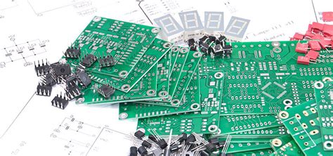
Dfm in pcb
Importance Of Design For Manufacturability (DFM) In PCB Production
Design for Manufacturability (DFM) is a critical aspect of printed circuit board (PCB) production that significantly influences the efficiency, cost-effectiveness, and quality of the final product. As the demand for more complex and compact electronic devices continues to rise, the importance of DFM in PCB production cannot be overstated. By integrating DFM principles early in the design process, manufacturers can anticipate potential production challenges and address them proactively, thereby streamlining the manufacturing process and reducing the likelihood of costly errors.
One of the primary benefits of implementing DFM in PCB production is the reduction of production costs.
By considering manufacturing constraints during the design phase, designers can optimize the layout and materials used, minimizing waste and ensuring that the design is compatible with existing manufacturing capabilities. This foresight not only reduces material costs but also shortens production time, as fewer design iterations are needed to achieve a manufacturable product. Consequently, companies can bring their products to market more quickly, gaining a competitive edge.
Moreover, DFM enhances the reliability and performance of PCBs.
By adhering to DFM guidelines, designers can ensure that the PCB layout is optimized for electrical performance, thermal management, and mechanical stability. This involves careful consideration of factors such as trace width, spacing, and layer stack-up, which are crucial for maintaining signal integrity and preventing issues like crosstalk and electromagnetic interference. Additionally, DFM encourages the use of standardized components and processes, which not only simplifies assembly but also improves the overall quality and consistency of the final product.
Transitioning from design to production, DFM plays a pivotal role in facilitating communication between design engineers and manufacturing teams.
By providing a common framework and language, DFM helps bridge the gap between these two critical functions, ensuring that design intentions are clearly understood and accurately translated into the manufacturing process. This collaboration is essential for identifying potential issues early on and implementing solutions that align with both design goals and manufacturing capabilities. As a result, the likelihood of encountering production delays or defects is significantly reduced.
Furthermore, DFM supports scalability and adaptability in PCB production.
As technology evolves and market demands shift, manufacturers must be able to quickly adapt their processes to accommodate new requirements. By incorporating DFM principles, companies can design PCBs that are not only manufacturable today but also adaptable to future advancements. This forward-thinking approach allows manufacturers to remain agile and responsive to changes in the industry, ensuring long-term success.
In addition to these practical benefits, DFM also contributes to sustainability in PCB production.
By optimizing designs for manufacturability, companies can reduce material waste and energy consumption, thereby minimizing their environmental impact. This aligns with the growing emphasis on sustainable practices within the electronics industry and meets the increasing demand from consumers for environmentally responsible products.
In conclusion, the importance of Design for Manufacturability in PCB production is multifaceted, encompassing cost reduction, enhanced reliability, improved communication, scalability, and sustainability. By integrating DFM principles into the design process, manufacturers can not only optimize their production processes but also deliver high-quality, reliable products that meet the evolving needs of the market. As the electronics industry continues to advance, the role of DFM in ensuring efficient and effective PCB production will undoubtedly remain indispensable.
Key DFM Guidelines For Optimizing PCB Layout
Design for Manufacturability (DFM) is a critical aspect of printed circuit board (PCB) design that ensures the transition from concept to production is as seamless as possible. By adhering to key DFM guidelines, designers can optimize PCB layouts to enhance manufacturability, reduce costs, and improve overall product quality. To begin with, understanding the importance of component placement is paramount. Proper component placement not only affects the electrical performance but also influences the ease of assembly and testing. Components should be arranged to minimize trace lengths, which reduces signal interference and potential crosstalk. Additionally, placing components with similar functions together can streamline the assembly process and facilitate easier troubleshooting.
Transitioning to the topic of trace routing, it is essential to maintain consistent trace widths and spacing to ensure signal integrity and prevent short circuits.
Designers should adhere to the manufacturer’s specifications for minimum trace width and spacing, which are often dictated by the capabilities of the fabrication process. Furthermore, employing a grid system for routing can help maintain uniformity and organization, making the layout more predictable and easier to manufacture. It is also advisable to avoid acute angles in trace routing, as these can lead to acid traps during the etching process, potentially causing defects.
Another crucial aspect of DFM is the consideration of thermal management.
As electronic devices become more compact and powerful, managing heat dissipation is increasingly important. Designers should strategically place thermal vias and heat sinks to facilitate efficient heat transfer away from critical components. Moreover, using copper pours and planes can help distribute heat more evenly across the PCB, reducing the risk of hotspots that could compromise performance or reliability.
In addition to thermal considerations, ensuring adequate spacing between components and traces is vital for manufacturability.
This spacing not only prevents electrical shorts but also allows for easier soldering and inspection. Designers should be mindful of the manufacturer’s capabilities regarding minimum spacing and adjust their layouts accordingly. Furthermore, incorporating test points into the design can greatly enhance the ability to perform in-circuit testing, ensuring that the PCB functions as intended before it is fully assembled.
Transitioning to the topic of material selection, choosing the right substrate material is another key factor in optimizing PCB layout for manufacturability.
The material should be compatible with the intended operating environment and capable of withstanding the thermal and mechanical stresses it will encounter. Additionally, the material’s dielectric properties should align with the electrical requirements of the design to ensure optimal performance.
Finally, collaboration with manufacturers during the design phase can provide valuable insights into the capabilities and limitations of the fabrication process.
By engaging in open communication with manufacturers, designers can receive feedback on their layouts and make necessary adjustments before production begins. This proactive approach can help identify potential issues early on, reducing the likelihood of costly revisions and delays.
In conclusion, adhering to key DFM guidelines is essential for optimizing PCB layouts and ensuring a smooth transition from design to production. By focusing on component placement, trace routing, thermal management, spacing, material selection, and collaboration with manufacturers, designers can create PCBs that are not only functional but also cost-effective and reliable. Through careful consideration of these factors, the manufacturability of PCBs can be significantly enhanced, ultimately leading to a more successful product development process.

Common DFM Mistakes In PCB Design And How To Avoid Them
Design for Manufacturability (DFM) is a critical aspect of printed circuit board (PCB) design that ensures a product can be manufactured with ease, efficiency, and cost-effectiveness. However, despite its importance, many designers often overlook certain DFM principles, leading to common mistakes that can complicate the manufacturing process. Understanding these pitfalls and learning how to avoid them is essential for optimizing PCB production.
One prevalent mistake in PCB design is neglecting to consider the manufacturer’s capabilities and limitations.
Each manufacturer has specific processes, materials, and technologies they specialize in, and failing to align the design with these can result in increased costs or production delays. To avoid this, designers should engage with manufacturers early in the design process, gaining insights into their capabilities and incorporating these into the design specifications. This collaboration ensures that the design is not only innovative but also manufacturable.
Another common error is inadequate spacing between components.
Insufficient spacing can lead to solder bridging, where solder unintentionally connects adjacent components, causing short circuits. To prevent this, designers should adhere to the manufacturer’s recommended spacing guidelines, which are typically based on their soldering technology and equipment. By doing so, the risk of defects during assembly is significantly reduced, enhancing the reliability of the final product.
Furthermore, improper layer stack-up is a frequent issue that can affect the electrical performance and manufacturability of a PCB.
A well-planned layer stack-up ensures signal integrity, minimizes electromagnetic interference, and facilitates efficient heat dissipation. Designers should carefully consider the arrangement of power, ground, and signal layers, consulting with manufacturers to ensure the stack-up aligns with their fabrication processes. This attention to detail can prevent costly redesigns and improve the overall performance of the PCB.
Additionally, overlooking the importance of thermal management is a mistake that can lead to overheating and failure of the PCB.
Effective thermal management involves the strategic placement of components, vias, and heat sinks to dissipate heat efficiently. Designers should conduct thermal simulations to identify potential hotspots and adjust the design accordingly. By prioritizing thermal management, the longevity and reliability of the PCB are significantly enhanced.
Moreover, inadequate documentation is a common oversight that can lead to miscommunication and errors during manufacturing.
Comprehensive documentation, including detailed schematics, assembly drawings, and a bill of materials, is crucial for ensuring that the manufacturer accurately interprets the design. Designers should strive to provide clear and concise documentation, regularly updating it to reflect any design changes. This practice minimizes the risk of errors and facilitates a smoother manufacturing process.
Lastly, failing to perform thorough design rule checks (DRC) is a mistake that can result in non-compliance with manufacturing standards.
DRCs are automated checks that verify the design against a set of predefined rules, identifying potential issues before fabrication. Designers should utilize DRC tools to ensure their design adheres to industry standards and the specific requirements of the manufacturer. By doing so, they can catch errors early, reducing the likelihood of costly revisions and production delays.
In conclusion, avoiding common DFM mistakes in PCB design requires a proactive approach that emphasizes collaboration with manufacturers, adherence to guidelines, and thorough verification processes. By understanding and addressing these potential pitfalls, designers can create PCBs that are not only innovative but also manufacturable, reliable, and cost-effective.
The Role Of DFM In Reducing PCB Manufacturing Costs
Design for Manufacturability (DFM) plays a pivotal role in the realm of printed circuit board (PCB) manufacturing, serving as a crucial strategy for reducing costs while maintaining high-quality standards. As the demand for more complex and compact electronic devices continues to rise, manufacturers are increasingly focusing on optimizing their processes to remain competitive. DFM, therefore, emerges as an essential approach that integrates design considerations with manufacturing capabilities, ultimately leading to cost-effective production.
To begin with, DFM involves a comprehensive analysis of the PCB design to ensure that it aligns with the manufacturing processes.
This alignment is critical because it helps in identifying potential issues that could arise during production, thereby allowing for preemptive adjustments. By addressing these issues early in the design phase, manufacturers can avoid costly rework and delays that often occur when problems are discovered later in the production cycle. Consequently, this proactive approach not only reduces manufacturing costs but also shortens the time-to-market for new products.
Moreover, DFM encourages collaboration between design engineers and manufacturing teams.
This collaboration is vital as it fosters a deeper understanding of the limitations and capabilities of the manufacturing processes. For instance, certain design features may be aesthetically pleasing or functionally desirable but could be challenging or expensive to produce. Through DFM, designers can receive feedback from manufacturers on how to modify these features to make them more manufacturable without compromising on performance. This iterative process ensures that the final design is both cost-effective and feasible to produce.
In addition to facilitating collaboration, DFM also emphasizes the importance of standardization in PCB manufacturing.
By adhering to industry standards and guidelines, manufacturers can streamline their processes, leading to more efficient production. Standardization reduces variability, which in turn minimizes the likelihood of defects and rework. This not only enhances the overall quality of the PCBs but also contributes to significant cost savings. Furthermore, standardized designs are often easier to scale, allowing manufacturers to meet increasing demand without incurring substantial additional costs.
Another critical aspect of DFM is the optimization of material usage.
By carefully selecting materials and components that are readily available and cost-effective, manufacturers can further reduce expenses. DFM encourages the use of materials that are not only economical but also compatible with existing manufacturing processes. This compatibility ensures that the production process is smooth and uninterrupted, thereby avoiding unnecessary costs associated with material shortages or substitutions.
Furthermore, DFM plays a significant role in enhancing the reliability and longevity of PCBs.
By incorporating design elements that facilitate easy assembly and testing, manufacturers can ensure that the final product meets the required quality standards. Reliable PCBs are less likely to fail, reducing the need for costly repairs or replacements. This reliability is particularly important in industries where PCBs are used in critical applications, such as aerospace or medical devices, where failures can have severe consequences.
In conclusion, the role of DFM in reducing PCB manufacturing costs cannot be overstated.
By integrating design and manufacturing considerations, fostering collaboration, emphasizing standardization, optimizing material usage, and enhancing reliability, DFM provides a comprehensive framework for cost-effective PCB production. As the electronics industry continues to evolve, the adoption of DFM principles will undoubtedly remain a key factor in achieving competitive advantage and ensuring sustainable growth.