Hdi full form in pcb
Understanding HDI: High-Density Interconnect in PCB Design
High-Density Interconnect (HDI) technology has become a cornerstone in the evolution of printed circuit board (PCB) design, playing a pivotal role in the advancement of modern electronics. As the demand for more compact, efficient, and powerful electronic devices continues to grow, HDI technology offers a solution by enabling the creation of smaller, lighter, and more efficient PCBs. Understanding the full form of HDI in the context of PCB design is essential for grasping its significance and the benefits it brings to the electronics industry.
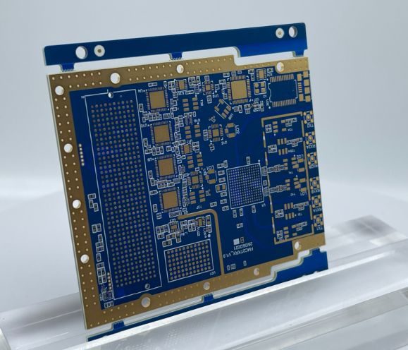
HDI, or High-Density Interconnect, refers to a type of PCB that incorporates a higher wiring density per unit area compared to traditional circuit boards.
This is achieved through the use of finer lines and spaces, smaller vias, and capture pads, as well as higher connection pad density. The primary advantage of HDI technology is its ability to accommodate more components in a smaller area, which is crucial for the miniaturization of electronic devices. As a result, HDI PCBs are widely used in applications where space and weight are critical factors, such as in smartphones, tablets, laptops, and other portable electronic devices.
The implementation of HDI technology in PCB design involves several advanced techniques, including the use of microvias, blind and buried vias, and sequential lamination.
Microvias are small-diameter vias that connect different layers of a PCB, allowing for more complex routing and increased layer density. Blind vias connect the outer layer to one or more inner layers without passing through the entire board, while buried vias connect inner layers without reaching the outer surfaces. These techniques enable designers to create multi-layer PCBs with intricate interconnections, thereby enhancing the functionality and performance of the final product.
Moreover, HDI technology supports the integration of advanced components such as fine-pitch ball grid arrays (BGAs) and chip-scale packages (CSPs), which are essential for high-performance applications.
The ability to incorporate these components into HDI PCBs allows for faster signal transmission, reduced power consumption, and improved thermal management. Consequently, devices utilizing HDI technology can achieve higher speeds and greater efficiency, meeting the ever-increasing demands of consumers and industries alike.
In addition to its technical advantages, HDI technology also offers economic benefits.
By reducing the size and weight of PCBs, manufacturers can lower material costs and improve production efficiency. Furthermore, the enhanced performance and reliability of HDI PCBs can lead to longer product lifespans and reduced maintenance costs, providing further value to both manufacturers and end-users.
Despite its numerous advantages, the adoption of HDI technology does present certain challenges.
The complexity of HDI PCB design requires specialized knowledge and expertise, as well as advanced manufacturing processes and equipment. Additionally, the cost of implementing HDI technology can be higher than that of traditional PCBs, particularly for low-volume production runs. However, as technology continues to advance and the demand for high-performance electronic devices grows, the benefits of HDI technology are likely to outweigh these challenges.
In conclusion, High-Density Interconnect technology represents a significant advancement in PCB design, offering a range of benefits that are essential for the development of modern electronic devices. By enabling the creation of smaller, more efficient, and more powerful PCBs, HDI technology is poised to play a crucial role in the future of electronics, driving innovation and meeting the evolving needs of consumers and industries worldwide.

The Role of HDI in Modern PCB Manufacturing
In the realm of modern electronics, the demand for more compact, efficient, and high-performing devices has led to significant advancements in printed circuit board (PCB) technology. One such advancement is the use of High-Density Interconnect (HDI) technology, which plays a pivotal role in the manufacturing of contemporary PCBs. HDI technology is characterized by its ability to incorporate more components in a smaller area, thereby enhancing the functionality and performance of electronic devices.
The full form of HDI in the context of PCB manufacturing is High-Density Interconnect.
This technology is distinguished by its use of finer lines and spaces, smaller vias, and capture pads, as well as higher connection pad density. These features enable the creation of more complex and compact circuit designs, which are essential for the miniaturization of electronic devices. As consumer electronics continue to shrink in size while increasing in capability, HDI technology has become indispensable in meeting these evolving demands.
One of the primary benefits of HDI technology is its ability to support higher wiring density.
This is achieved through the use of microvias, which are significantly smaller than traditional vias. Microvias allow for more interconnections within a given area, facilitating the design of multi-layer PCBs with more intricate circuitry. This increased density is crucial for modern applications, such as smartphones, tablets, and wearable devices, where space is at a premium and performance cannot be compromised.
Moreover, HDI technology contributes to improved signal integrity and reduced signal loss.
The shorter distances between components and the use of advanced materials help minimize the potential for signal degradation, which is particularly important in high-speed applications. As electronic devices become more sophisticated, the need for reliable and efficient signal transmission becomes paramount. HDI PCBs address this need by providing a robust platform for high-frequency and high-speed data transmission.
In addition to enhancing performance, HDI technology also offers significant advantages in terms of design flexibility.
The ability to incorporate more components and connections in a smaller area allows designers to explore innovative configurations and functionalities. This flexibility is particularly beneficial in the development of cutting-edge technologies, such as 5G networks, Internet of Things (IoT) devices, and advanced automotive systems. By enabling more complex designs, HDI technology supports the continuous evolution of electronic devices and systems.
Furthermore, the use of HDI technology can lead to cost savings in the long run.
Although the initial manufacturing costs may be higher due to the complexity of the processes involved, the overall cost-effectiveness is realized through the reduction in material usage and the potential for increased product lifespan. The ability to integrate more functions into a single PCB reduces the need for additional components and assemblies, ultimately leading to a more streamlined and efficient production process.
In conclusion, the role of High-Density Interconnect technology in modern PCB manufacturing is both significant and transformative.
By enabling higher component density, improved signal integrity, and greater design flexibility, HDI technology addresses the challenges posed by the ever-increasing demand for smaller, faster, and more efficient electronic devices. As the electronics industry continues to advance, the importance of HDI technology in shaping the future of PCB manufacturing cannot be overstated.
Advantages of Using HDI Technology in PCB Development
High-Density Interconnect (HDI) technology in Printed Circuit Board (PCB) development represents a significant advancement in the electronics industry, offering numerous advantages that cater to the ever-evolving demands for more compact, efficient, and powerful electronic devices. As the name suggests, HDI technology allows for a higher density of interconnections on a PCB, which is achieved through the use of finer lines and spaces, smaller vias, and capture pads, as well as higher connection pad density. This technological innovation is particularly beneficial in the context of modern electronic devices, which require increasingly sophisticated and compact designs.
One of the primary advantages of HDI technology is the ability to significantly reduce the size and weight of electronic devices.
As consumer electronics continue to trend towards smaller and more portable designs, the need for compact PCBs becomes increasingly critical. HDI technology enables the miniaturization of PCBs without compromising functionality or performance. By utilizing microvias, blind vias, and buried vias, HDI PCBs can accommodate more components in a smaller area, thus allowing for the development of sleeker and lighter devices. This is particularly advantageous in the production of smartphones, tablets, and wearable technology, where space is at a premium.
In addition to size reduction, HDI technology enhances the performance and reliability of PCBs.
The increased density of interconnections allows for shorter signal paths, which in turn reduces signal loss and improves signal integrity. This is crucial in high-speed applications where maintaining signal quality is paramount. Furthermore, the use of microvias in HDI PCBs reduces parasitic capacitance and inductance, which can adversely affect the performance of high-frequency circuits. As a result, HDI technology is well-suited for applications that require high-speed data transmission and processing, such as telecommunications and computing.
Moreover, HDI technology facilitates the integration of advanced features and functionalities into electronic devices.
The ability to incorporate more components into a smaller area allows designers to add new features without increasing the overall size of the device. This is particularly beneficial in the development of multifunctional devices that combine various capabilities into a single unit. For instance, modern smartphones often integrate cameras, GPS, and various sensors, all of which require additional circuitry. HDI technology makes it possible to accommodate these components without compromising the device’s form factor.
Another significant advantage of HDI technology is its contribution to improved thermal management.
As electronic devices become more powerful, they generate more heat, which can negatively impact performance and longevity. HDI PCBs, with their compact design and efficient use of space, allow for better heat dissipation. The shorter interconnection paths and smaller vias reduce thermal resistance, enabling more effective heat transfer away from critical components. This is particularly important in high-performance applications where thermal management is a key consideration.
In conclusion, HDI technology in PCB development offers a multitude of advantages that address the growing demands for smaller, more efficient, and more powerful electronic devices. By enabling size reduction, enhancing performance and reliability, facilitating feature integration, and improving thermal management, HDI technology plays a crucial role in the advancement of modern electronics. As the industry continues to evolve, the adoption of HDI technology is likely to become increasingly widespread, driving further innovation and development in the field of electronics.
HDI vs. Traditional PCB: Key Differences and Benefits
High-Density Interconnect (HDI) technology represents a significant advancement in the field of printed circuit boards (PCBs), offering numerous advantages over traditional PCB designs. As electronic devices continue to shrink in size while increasing in functionality, the demand for more compact and efficient circuit boards has grown. HDI technology addresses this need by enabling the creation of smaller, lighter, and more powerful PCBs, which are essential for modern electronic devices.
One of the primary differences between HDI and traditional PCBs lies in the density of the interconnections.
HDI PCBs are characterized by their use of microvias, blind vias, and buried vias, which allow for a higher density of connections within a smaller area. This contrasts with traditional PCBs, which typically rely on through-hole vias that require more space and limit the potential for miniaturization. The use of microvias in HDI PCBs not only reduces the overall size of the board but also enhances its electrical performance by shortening the signal paths, thereby reducing signal loss and improving signal integrity.
Moreover, HDI technology facilitates the integration of more components on a single board.
This is particularly beneficial in applications where space is at a premium, such as in smartphones, tablets, and other portable electronic devices. By enabling a higher component density, HDI PCBs support the development of more complex and feature-rich devices without compromising on size or weight. This capability is a significant advantage over traditional PCBs, which may require multiple layers and larger board sizes to accommodate the same number of components.
In addition to size and component density, HDI PCBs offer improved thermal management compared to their traditional counterparts.
The increased number of interconnections and the use of advanced materials in HDI designs allow for more efficient heat dissipation, which is crucial for maintaining the reliability and longevity of electronic devices. This is particularly important in high-performance applications where excessive heat generation can lead to component failure or reduced performance.
Furthermore, the manufacturing process for HDI PCBs is more advanced and precise, allowing for tighter tolerances and more intricate designs.
This precision is essential for producing the fine features required in modern electronics, such as narrow traces and small pads. While the manufacturing process for HDI PCBs can be more complex and costly than that of traditional PCBs, the benefits in terms of performance, size, and functionality often outweigh these considerations.
Despite the advantages of HDI technology, it is important to note that traditional PCBs still have their place in the industry.
For applications where size and weight are not critical factors, or where cost is a primary concern, traditional PCBs may still be the preferred choice. However, as the demand for smaller, more powerful electronic devices continues to grow, the adoption of HDI technology is likely to increase.
In conclusion, HDI technology offers several key benefits over traditional PCB designs, including higher interconnection density, improved electrical performance, enhanced thermal management, and the ability to support more complex and compact devices. As electronic devices continue to evolve, the role of HDI PCBs in enabling these advancements will become increasingly important, making them a critical component in the future of electronics manufacturing.