Heavy Copper PCB
Rich experience in heavy copper PCB
LJL~`{%HC_6KJ5TIN@~5V")
The additional copper PCB thickness enables the board to conduct a higher current, achieve good thermal distribution and implement complex switches in a limited space.
Other advantages include increased mechanical strength at connector sites, the ability to create a smaller product size by incorporating multiple weights on the same layer of circuitry and the ability to use exotic materials to their maximum capacity with minimal risk of circuit failure.
[`](V")
Heavy Copper PCB Stack Up
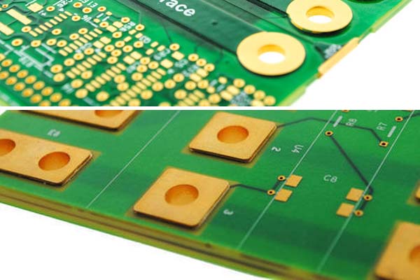
Heavy copper usually means the copper foil thickness of PCB higher than 3 ounce (4 mil or 100 micron). It can be design in inner layer or outer layer.
In PCB production, it is more difficult than traditional circuits with copper foil less than 2 ounce.

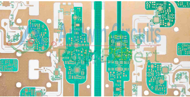
Heavy copper PCB section
How Are Heavy Copper PCBs Made?
Andwin utilizes a unique process referred to as “Laminated Deposition”.
This combination of processes allows extreme copper thickness requirements to become very practical and cost effective.
The process utilizes heavy base copper that delivers consistent and reliable high power circuits when placed in our plating and etching systems, allowing us to produce well-defined track edges, finer lines, and finer spaces.
Heavy Copper PCB’s Capabilities
Based on the requirement, heavy copper PCBs can be expensive to produce.
Thus, it is more complex in design but more effective in producing heavy copper PCB.
It should have the following capabilities:

Heavy Copper PCB’s Benefits
Heavy Copper PCB Are Useful For Multiple Purposes :

If you got questions about our Thick Copper PCB manufacturing capabilities or your custom project required specifications are not listed in this page, reach us at anytime. We will reply within 3 hours.
