Power Path Controller System Using LTC4412 to Implement Primary and Secondary Power Switching
Power Path Controller System Using LTC4412 to Implement Primary and Secondary Power Switching
In many cases, our circuit design has two power sources like adapter and battery, or it can even be two other power sources from two different sockets. The requirement of the application may be such that during power failure, it should always need to remain on by using the available extra power. For example, a circuit powered by an adapter needs to switch to the battery or auxiliary power in case of power failure without interrupting the operation of the circuit.
In the above cases, the power path controller circuit will be helpful. Basically, the power path control circuit will switch the main power supply of the board according to the available power supply by controlling the path of the power entering the circuit.
In this project, we will build a dedicated power path controller system to switch the power input of the load from the primary power supply to the auxiliary power supply when the main power fails, and switch the auxiliary power supply to the primary power supply again during the main power recovery phase. This is a necessary circuit to support the uninterruptible power supply application state during the process of input power changing from primary power supply to auxiliary power supply or auxiliary power supply to primary power supply. In other words, it can work like a UPS for Arduino and Raspberry Pi projects, and can also charge multiple batteries with one charger.

Requirements
The requirements of the circuit are specified as follows
- The load current will be 3A.
- The maximum voltage of the adapter (primary power source) is 12V and the maximum voltage of the battery (secondary power source) is 9V.
LTC4412 Power Path Controller
The primary controller selected for the circuit is the LTC4412 from Analog Devices (Linear Technology). This is a low-loss power path controller system that automatically switches between two DC power sources, simplifying load sharing operations. Since this device supports adapter voltages ranging from 3V to 28V and supports battery voltages ranging from 2.5V to 25V. Therefore, it meets the above input voltage requirements. The pin diagram of the LTC4412 is shown in the figure below.
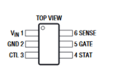
However, it has two input sources, one is the primary power source and the other is the auxiliary power source.
The primary power source (in this case, the wall adapter) takes precedence over the auxiliary power source (in this case, the battery). Therefore, whenever the primary power source is present, the auxiliary power source will automatically disconnect. The difference between these two input voltages is only 20mV. So if the primary supply is 20mV higher than the auxiliary supply, the load is connected to the primary supply.
The LTC4412 has two additional pins – control and status.
The control pin can be used as a digital control input to force the MOSFET to turn off, while the status pin is an open drain output pin that can be used to sink 10uA of current and can be used to control an additional MOSFET with an external resistor. This can also be interfaced with a microcontroller to get the presence signal of the auxiliary supply. The LTC4412 also provides reverse polarity protection for the battery. But since we are working with power supplies, here you can also check out other designs like overvoltage protection, overcurrent protection, reverse polarity protection, short circuit protection, hot swap controllers, etc., which may come in handy
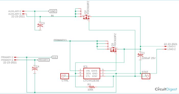
Another component is the use of two p-channel mosfets to control the auxiliary and primary supplies. For this purpose, the FDC610PZ is used as the P-channel, -30V, -4.9A MOSFET, which is suitable for 3A load switching work. It has a low RDSON resistance of 42 milliohms, which makes it suitable for such applications without the need for an additional heat sink.
Therefore, the detailed BOM code is-
- LTC4412
- P-channel MOSFET- FDC610PZ – 2pcs
- 100k resistor
- 2200uF capacitor
- Connector – 3pcs
- PCB
LTC4412 Power Path Controller Circuit Diagram
The circuit has two operating states, one is primary power loss and the other is primary power recovery. The main work is done by the controller LTC4412. When the main power supply voltage is 20mv lower than the auxiliary power supply voltage, the LTC4412 connects the output load with the auxiliary power supply. In this case, the state pin sinks current and turns on the auxiliary MOSFET.
Under other operating conditions, each time the main power input is 20mv higher than the auxiliary power supply, the load is connected to the main power supply again. The state pin then enters the open drain state and will turn off the p-channel MOSFET.
These two conditions can not only automatically switch the power supply according to the primary power failure, but also switch when the primary voltage drops significantly.
If VIN does not get any voltage, the sense pin provides power to the internal circuitry and also senses the voltage of the main power supply unit.
The larger output capacitor of 2200uF 25V will provide adequate filtering during the switch off phase. The capacitor will provide power to the load during the small duration when the switching occurs.
PCB Board Design
To test the circuit, we need a PCB as the LTC4412 IC is in an SMD package. In the image below, the top side of the board is shown-
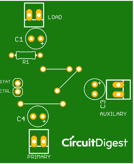
The design is done as a single sided board. 3 jumpers are also required in the PCB. Two more optional input and output pins are provided for control and status related operations. If required, the microcontroller unit can be interfaced in these two pins but we will not do that in this tutorial.

In the above image, two mosfets of Q1 and Q2 are shown at the bottom of the PCB. However, the mosfets do not require an additional heat sink but in the design, a PCB heat sink is created. This will reduce the power dissipation of the entire mosfets.
Power Path Controller Testing
The above two images show the PCB of the power path controller designed earlier. However, the PCB is a hand-etched version which will serve the purpose. The components on the board are soldered correctly.
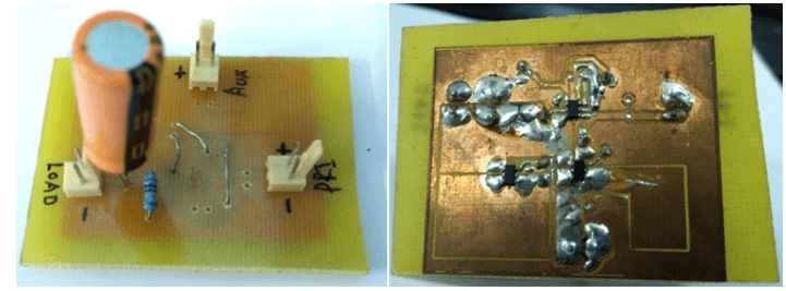
To test the circuit, an adjustable DC load that draws nearly 1 amp is connected at the output. If you don’t have a digital DC load, you can also build your own adjustable DC load using Arduino.

For testing purposes, I faced a battery shortage (COVID-19 lockdown here) and so used a bench power supply with two outputs. One channel was set to 9V and the other to 12V. Disconnect the 12V channel to see the output results and reconnect the channel to check the performance of the circuit.