There is a black thing on the PCB circuit board. Do you know what it is?
1.What is COB soft package
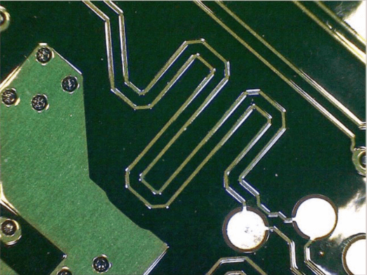
Careful netizen may find that there is a black thing on some circuit boards. What is this thing? Why is it on the circuit board? What is its function? In fact, this is a kind of package. We often call it “soft package”. It is called soft package for “hard”. Its composition material is epoxy resin. We usually see that the receiving surface of the receiving head is also this material.
It contains chip IC. This process is called “bonding”, which we usually call “binding”.
This is a wire bonding process in the chip production process. Its English name is COB (Chip On Board), which is chip on board package. This is one of the bare chip mounting technologies. The chip is mounted on the PCB printed circuit board using epoxy resin. So why do some circuit boards not have this package? What are the characteristics of this package?
2.Characteristics of COB soft packaging
This soft packaging technology is often used for cost. As the simplest bare chip mounting, in order to protect the internal IC from damage, this package generally requires one-time molding. It is generally placed on the copper foil surface of the circuit board. The shape is round and the color is black. This packaging technology has the advantages of low cost, space saving, thinness, good heat dissipation, and simple packaging method. Many integrated circuits, especially most low-cost circuits, use this method to lead out multiple metal wires on the integrated circuit chip, and then hand it over to the manufacturer to put the chip on the circuit board, weld it with a machine, and then apply glue to cure and harden.
3.Application occasions
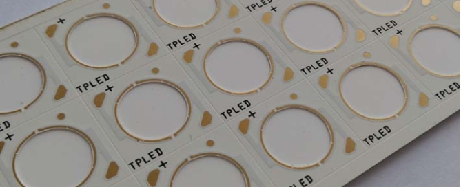
This package has its own unique characteristics. Therefore, in some electronic circuits, such as MP3 players, electronic pianos, digital cameras, game consoles, etc., some circuits that pursue low cost also use this package. In fact, COB soft packaging is not limited to chips, but also widely used in LEDs, such as COB light source, which is an integrated surface light source technology that directly attaches the LED chip to the mirror metal substrate.

4.The specific process flow of COB packaging is as follows:
(1) Chip preparation: First, you need to select a suitable chip, clean and inspect it to ensure that there are no contaminants and defects on the chip surface.
(2) Chip pasting: On the prepared PCB, use conductive glue or thermal conductive glue to paste the chip to the specified position. This requires high-precision positioning and correct control of the glue.
(3) Gold wire connection: Use micro-wire bonding or wire bonding machine to connect the gold wires on the chip to the pins on the PCB. These gold wires play the role of signal transmission and electrical connection.
(4) Package curing: Through thermal curing or UV curing glue, the chip is tightly connected to the PCB and ensures stability and reliability.
(5) Package protection: In order to protect the chip and connecting wires, epoxy resin or other protective materials are usually used for coating after packaging.
Compared with traditional packaging technology, COB packaging has many significant advantages.
First, since the chip is directly mounted on the PCB, the package volume can be significantly reduced, and the integration and space utilization can be improved.
Secondly, COB packaging does not require solder pins or pins, which can reduce resistance and inductance, improve electrical performance and signal transmission speed. In addition, the direct connection method of COB packaging reduces the failure points of pins and welding, and improves reliability and durability.
COB packaging is widely used in electronic devices that require high performance and small size, especially mobile devices, communication equipment and consumer electronics. It can achieve a more compact and lightweight design and provide higher integration and reliability. However, COB packaging also faces some challenges, such as high requirements for precision positioning and fine craftsmanship, and sensitivity to factors such as temperature and humidity in the production environment.
5.Advantages of COB process
(1) COB packaging process has better protection
If ordinary LED displays are subjected to large external forces during transportation or installation, individual lamp beads or welding may fall off, which will cause some dots to be damaged, not glow, or display in monochrome, which is closely related to the packaging process. The introduction of COB packaging has greatly improved this phenomenon, because COB packaging directly packages the LED chip in the concave lamp slot of the PCB board and then fixes it with epoxy resin, so the entire lamp ball is a convex spherical surface, which is smooth and hard as a whole, so the protection performance is better.
(2) The dot pitch of COB packaging process is smaller
The COB packaging process can reduce the dot pitch of LED lamp beads. The original SMD packaged LED display dot pitch can only be about P1.3. It is difficult to achieve a lower dot pitch and it is impossible to guarantee a certain range of dead lights. COB packaging changes the arrangement and composition of LED lamp beads, so its dot pitch can be made smaller in essence, such as P2, P0.9 and other models.
(3) COB packaging process has fewer bad lamps and longer life
Because COB packaging technology products are to package the lamp on the PCB board, the heat of the lamp core is quickly transferred out through the copper foil on the PCB board, and the thickness of the copper foil on the PCB board has strict process requirements. In addition, the lean process will not cause excessive light attenuation, so there are few bad lamps, which greatly extends the service life of the LED display.
6.Disadvantages of COB process
(1) COB packaging process is difficult to produce
When COB packaging is used for LED display, it is necessary to ensure that each lamp is in good condition before the glue is filled. Unlike SMD packaging, which can replace a lamp bead individually, the requirements for the entire packaging process are very high, so it is difficult to produce and its price is also much higher.
(2) Inconvenient maintenance of COB packaging process
For traditional SMD packaging, if a LED display has a bad light, the unit board can be removed and the single light bead can be repaired by welding. However, if the COB packaged product is repaired in this way, it will affect the surrounding lights, so the maintenance is more difficult. Although the protection performance of COB packaging is better, there will still be a certain number of bad lights, but the failure rate is lower, and in this case, only a set of unit PCB boards can be replaced.