How to do ceramic pcb assembly?
What is ceramic pcb assembly?
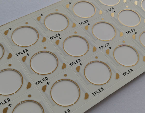
Ceramic PCB assembly refers to the process of assembling electronic components
onto a ceramic printed circuit board (PCB). Ceramic PCBs are made of a ceramic material,
such as aluminum oxide (Al2O3) or aluminum nitride (AlN), which offers excellent
thermal conductivity and electrical insulation properties.
During the assembly process, electronic components such as resistors, capacitors,
integrated circuits, and connectors are soldered onto the ceramic PCB using various
methods such as surface mount technology (SMT) or through-hole technology (THT).
The components are carefully placed and soldered onto the PCB to create a
functional electronic circuit.
Ceramic PCB assembly is commonly used in applications that require high power
handling, high-frequency performance, and excellent thermal management. These
include power electronics, LED lighting, aerospace and defense systems, automotive
electronics, and telecommunications equipment. The use of ceramic PCBs helps to
dissipate heat efficiently, improve reliability, and enhance the overall performance
of electronic devices.

How to do ceramic pcb assembly?
Ceramic PCB assembly is a specialized process that requires careful handling
and attention to detail. Here are the steps involved in ceramic PCB assembly:
1. Component selection: Choose the appropriate components for your ceramic
PCB assembly. Ensure that the components are compatible with ceramic substrates
and can withstand high temperatures.
2. PCB design: Create a PCB layout that accommodates the ceramic substrate
and the components. Pay attention to the thermal management aspects to ensure
efficient heat dissipation.
3. Solder paste application: Apply solder paste to the ceramic substrate using
a stencil or a dispenser. Ensure that the solder paste is evenly distributed and of the right thickness.

4. Component placement: Carefully place the components onto the solder
paste on the ceramic substrate. Use a pick-and-place machine or manual
placement depending on the complexity of the assembly.
5. Reflow soldering: Transfer the ceramic PCB to a reflow oven or a reflow
soldering machine. The oven will heat the assembly to the required temperature,
melting the solder paste and forming strong electrical connections.
6. Inspection: After the reflow soldering process, inspect the ceramic PCB
assembly for any defects or soldering issues. Use visual inspection techniques
or automated inspection systems to identify and rectify any problems.

7. Testing: Once the inspection is complete, test the ceramic PCB assembly to
ensure that it meets the required specifications and functions correctly. Use
appropriate testing equipment and procedures to verify the functionality and performance of the assembly.
8. Cleaning: Clean the ceramic PCB assembly to remove any flux residues
or contaminants that may have accumulated during the assembly process.
Use a suitable cleaning solution and techniques that are compatible with ceramic substrates.
9. Final inspection and packaging: Perform a final inspection of the ceramic
PCB assembly to ensure that it meets all quality standards. Once approved,
package the assembly in suitable packaging materials to protect it during transportation and storage.
It is important to note that ceramic PCB assembly requires specialized equipment,
expertise, and knowledge of the unique characteristics of ceramic substrates.
It is recommended to work with experienced PCB assembly service providers or
consult experts in ceramic PCB assembly to ensure a successful and reliable assembly process.
