How do rule settings apply to my PCB design?
In PCB design, Design Rule is the key to the success or failure of a PCB design. All the intentions of designers and the functional embodiment of the design are driven and realized through the soul of design rules. Exquisite and meticulous rule definitions can help designers to be handy in the work of PCB layout and routing, save a lot of energy and time of engineers, help designers to achieve excellent design intentions, and greatly facilitate the design work.
In PCB design, Design Rule is the key to the success or failure of a PCB design.
All the intentions of designers and the functional embodiment of the design are driven and realized through the soul of design rules. Exquisite and meticulous rule definitions can help designers to be handy in the work of PCB layout and routing, save a lot of energy and time of engineers, help designers to achieve excellent design intentions, and greatly facilitate the design work.
After the design data is transferred from the schematic stage to the PCB design stage, when performing PCB design layout and routing, it is necessary to define the design rules in advance.
The entire subsequent PCB design needs to comply with the rule definition. Including the most basic electrical rules (spacing, short circuit and open circuit), wiring rules (line width, routing style, via style, fan-out, etc.), plane rules (power ground plane layer connection method, copper connection method); and other commonly used auxiliary rules such as layout rules, manufacturing rules, high-speed design rules, signal integrity rules, etc. After the rule-driven design is completed, you can also perform a rule check Design Rule Check to review your design to see if there are any violations of the rules and make improvements and improvements. Finally, an excellent work that fully complies with the rule definition and meets the design intent is designed.
Design rules related to PCB manufacturing are particularly practical.
If the design rules are not set to meet the requirements of PCB process manufacturing, it will not only affect the product function, but may even fail to process and fail to achieve the engineer’s design intent. Therefore, when defining design rules, it is crucial to understand the downstream manufacturer’s process manufacturing requirements for the design.
What are the precision requirements for the manufacturing process of PCB processing?
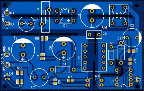
The following figure shows the process requirements of a PCB plate manufacturer. Including basic parameter requirements such as the number of circuit board layers, thickness, aperture, minimum line width and line spacing, copper thickness; also including special requirements such as board type, surface treatment, special processing, etc. Generally, when processing PCB, it is divided into proofing processing for testing and batch product processing for final molding. For designers, the process requirements for batch product processing are of practical significance and need to be strictly followed.
As for the process requirements related to manufacturing accuracy, the most basic and important are line width, line spacing and minimum aperture. That is, the minimum line width and the minimum hole size that the processing plant can handle. If the line width does not meet the requirements in the design, it cannot be processed correctly if it is too thin. The accuracy of line width and line spacing also affects whether the text pattern on the silk screen layer is clear. If the aperture is too small, there is no corresponding drill bit support. The drill bit size corresponding to the minimum aperture also affects the tolerance accuracy of various types of plate shearing such as mechanical holes and mounting holes.

Notes on setting line width, line spacing and aperture rules
This article will show you how to set line width, line spacing and aperture rules that meet the requirements and design intent in terms of PCB manufacturing accuracy according to the requirements of PCB manufacturing process.
Minimum line width/spacing 4mil
In PCB design, the highest accuracy that batch processing can support is line width and line spacing of 4mil. That is, the wiring width must be greater than 4mil, and the spacing between two lines must also be greater than 4mil. Of course, it is only the minimum limit of line width and line spacing. In actual work, the line width needs to be defined as different values according to design needs. For example, the power network is defined wider and the signal line is defined thinner. These different requirements can be defined in the rules Design – Rules – Routing – Width to define different line width values for different networks, and then set the rule application priority according to the importance. Similarly, for line spacing, define the electrical safety spacing between different networks in the rules page Design – Rules – Electrical – Clearance, of course, including line spacing.
There is also a special case.
For components with high-density pins, the spacing between pads in the device is generally very small, such as 6mil. Although it meets the manufacturing requirements of minimum line width or spacing greater than 4mil, it may not meet the rule design requirements for designing PCB. If the minimum safe spacing setting of the entire PCB is 8mil, then the spacing of the component pads obviously violates the rule setting. During rule checking or online editing, it will always be highlighted in green to show the violation. This violation obviously does not need to be handled, and we should correct the rule settings to eliminate the green highlight. In the original solution, different safe spacing rules were defined for this device separately in query language and set to high priority. In the new version, you only need to simply check the option to solve this problem, that is, Ignore Pad to Pad clearance within a footprint. As shown in the figure below.
It is very easy to check this option. There is no need to use the query statement InComponent(‘U1’) as before, and then set its minimum safe spacing to 6mil and set it as the highest spacing priority.
2.Minimum mechanical aperture 0.2mm (8mil) Minimum laser aperture 4mil
Drilling is inevitable in PCB design. In terms of setting design rules, or even specific drilling operations, do you know what kind of holes to drill (through holes, blind holes, buried holes, or back drilling holes?) and what size of holes to drill? Will you drill the same size of holes as others, or fill in a size at random to meet the convenience of board layout and routing?
The types of holes are shown in the figure below. Generally, through holes are usually used in designs that are not too complicated and have few board layers. In complex designs, especially multi-layer boards, high-speed and high-density designs, and when PCB wiring space requirements are very high, blind holes or buried holes can be set according to actual needs. Of course, blind and buried holes are more complicated in manufacturing process than through holes, and the manufacturing cost will increase accordingly.
Difference between mechanical drilling and laser drilling
First, let’s understand the drilling process. As shown in the figure below, drilling is done with drill bits of different specifications. If the size of the via hole in your design is different from the existing drill bit size in the processing plant, the drill bit specification closest to your design value will be selected for drilling. The Entry panel is used to protect the drill bit and the table, reduce burrs and reduce the temperature of the drill bit. The Backup base plate is used to protect the board surface from indentation, prevent slipping and reduce burrs.
Mechanical drilling drill bits are usually ST and UC. Generally speaking, UC drilling has higher drilling accuracy than ST.
Laser drilling is generally used for micro-vias. As PCBs develop in the direction of micro- and high-density interconnection, more and more board processing uses guide hole connection to achieve high-density interconnection. The small hole capacity of traditional mechanical drilling has almost reached its limit. With the development of blind hole design, the demand for high density also requires new processes to improve its reliability, and laser drilling has come into being. The following figure shows the method of laser drilling.
Therefore, the difference between mechanical drilling and laser drilling is as follows:
The accuracy of laser drilling is much higher than that of mechanical drilling. Therefore, the minimum mechanical drilling aperture must not be less than 0.2mm (8mil) in the rule setting. The minimum laser aperture must not be less than 4mil in the rule setting.
3.Relationship between aperture setting and board thickness, number of layers, etc.
The aperture setting size is first determined based on the accuracy required by the board, board thickness, number of layers, etc., while meeting the minimum process requirements. The relationship between them is as follows:
Therefore, when setting the aperture size, you can refer to the table above to set the corresponding size that meets the requirements according to the board thickness, number of layers, etc. You can also use the following simple board thickness/aperture ratio to roughly define the appropriate drilling aperture size based on the entire board thickness size.