Optimizing PCB Layout for High Speed ADC Design
High speed design is often overlooked or quite important. System board layout has become a major part of the design itself, so we must understand the mechanisms that affect the performance of high speed signal chain designs.
As engineers, we are also likely to “make” more trouble. Therefore, it is important not to be too picky and put the CAD engineer in a design dilemma, which will not bring any improvement in performance.
Don’t forget the exposed pad
The exposed pad is sometimes overlooked, but it is very important to fully utilize the signal chain performance and help the device heat dissipation. The exposed pad, which we usually call Pin 0 at Analog Devices, is the pad on the bottom of most devices today. It is an important connection point, and all the internal grounds of the chip are connected to the center point under the device through it.
Have you noticed that many converters and amplifiers today are missing a ground pin?
The exposed pad is the reason. It is critical to properly fix (i.e. solder) this pin to the printed circuit board (PCB) to achieve a robust electrical and thermal connection, otherwise, the system design may be damaged in various ways.
There are basically three steps to achieve the best electrical and thermal connection using the exposed pad.
First, replicate the exposed pad on each layer of the PCB, whenever possible. This will provide a thick thermal connection to all grounds and ground planes for quick heat dissipation.
This step is relevant for high-power devices and applications with multiple channels. Electrically, this will provide a good equipotential connection for all ground planes. You can even replicate the exposed pad on the bottom layer (Figure 1), which can serve as a thermal pad ground point for decoupling and a location to mount a bottom-side heat sink.
Replicating the exposed pad on each layer can help create a robust electrical and thermal ground connection
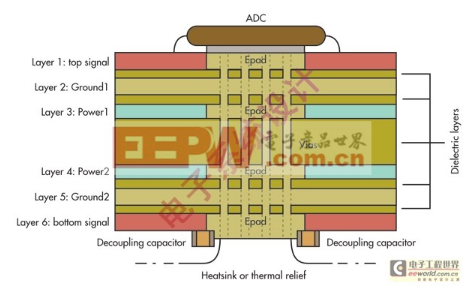
Figure 1: Replicating the exposed pad on each layer can help create a robust electrical and thermal ground connection, while also adding additional area for thermal pads and bottom-side decoupling.
Second, segment the exposed pad into multiple identical sections like a chessboard. This can be done in two ways: using silkscreen cross-hatching or solder mask on the open exposed pad. This step ensures a robust connection between the device and the PCB. During the reflow assembly process, there is no way to determine how the solder paste will flow and ultimately connect the device to the PCB.
If the exposed pad is not segmented and the vias are not filled, voids will form during the reflow process
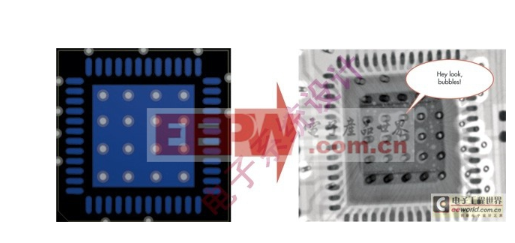
Figure 2: If the exposed pad is not segmented and the vias are not filled, voids will form during the reflow process.
The problem is that the connection may exist but it is not evenly distributed. You may only get one connection and it may be small, or worse, it may be in a corner. Segmenting the exposed pad into smaller sections ensures that each area has a connection point, resulting in a more robust, evenly connected exposed pad (Figures 2 and 3).
Segmenting the exposed pad on the PCB helps the PCB and IC bond more tightly during the board assembly process
Figure 3: Segmenting the exposed pad on the PCB helps the PCB and IC bond more tightly during the board assembly process.
Finally, you should ensure that each section has a via connected to ground. Each area is usually large enough to place multiple vias. Before assembly, it is important to fill each via with solder paste or epoxy. This step is very important to ensure that the exposed pad solder paste does not flow back into these via holes and reduce the chance of a proper connection.
Decoupling and Plane Capacitance
Sometimes we forget the purpose of using decoupling and simply spread many values of capacitors on the board to connect the lower impedance power supply to ground. But the question remains: how many capacitors are needed?
Many literatures indicate that multiple capacitors and multiple values should be used to reduce the impedance of the power delivery system (PDS), but this is not entirely correct. In fact, just choosing the right value and the right “type” of capacitor can reduce the impedance of the PDS.
For example, if we want to design a 10mΩ reference plane, if we use multiple capacitor values on the system board, we can reduce the impedance in the 500MHz frequency range, as shown by the red curve in Figure 4.
Standard decoupling capacitors can help reduce PDS impedance up to 500MHz
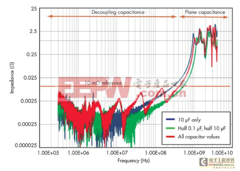
Figure 4: Standard decoupling capacitors can help reduce PDS impedance up to 500MHz, while planar capacitors take care of frequencies above 500MHz. Understanding the capacitors used can reduce the number and type of capacitors used in a design.
However, let’s look at the green curve again, which only uses 0.1μF and 10μF capacitors on the same design. This proves that if the right capacitors are used, there is no need to use so many capacitor values. This can also help save layout and bill of materials (BOM) costs.
However, not all capacitors are “created equal” and even from the same supplier, they have different processes, sizes and styles. If the correct capacitors are not used, whether multiple capacitors or several different types of capacitors are used, the result will be counterproductive to the PDS.
Placing capacitors or using different capacitor processes and types can create inductive loops that will respond differently to frequencies within the system and resonate with each other (Figure 5).
It is important to understand the frequency response of the type of capacitors used in the system. Choosing capacitors haphazardly will undo the effort of designing a low impedance PDS system.
To design a good PDS, a variety of capacitors are used (see Figure 4 again). Typical capacitor values used on the PCB will only reduce impedance within a frequency range of about 500MHz at or near DC. Above 500MHz, the capacitance will be determined by the internal capacitance formed by the PCB. Are the power and ground planes stacked closely enough?
To do this, design a PCB stackup that supports large planar capacitance. For example, a six-layer stackup might include the top signal layer, the first ground layer, the first power layer, the second power layer, the second ground layer, and the bottom signal layer. Specify that the first ground layer and the first power layer are close to each other in the stackup. Setting the spacing between these two layers to 2-4 mils will form an inherent high-frequency planar capacitance.
Loop inductance can be minimized through capacitor type and layout
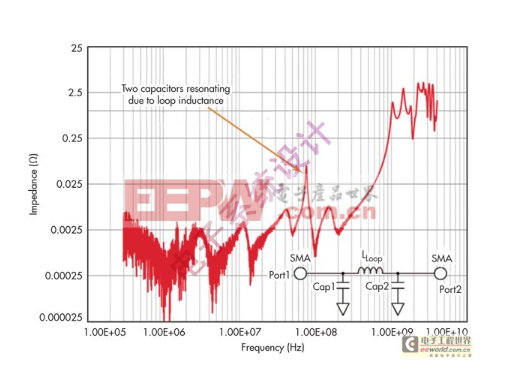
Figure 5: By understanding capacitor type and layout, loop inductance can be minimized, preventing high PDS impedance.
The best thing about this capacitor is that it is free and you only need to account for it in your PCB manufacturing notes. If you must split the power plane and have multiple VDD rails on the same plane, use the largest possible power plane. Do not leave voids and be mindful of sensitive circuits. This will maximize the capacitance of that VDD plane.
If the design allows for additional layers (eight in this case, instead of six), two additional ground planes should be placed between the first and second power planes. With the same 2-3 mil core spacing, the inherent capacitance of the stack-up will double (Figure 6). This structure is easier to design, and then more discrete high-frequency capacitors can be added to keep impedance low.
By designing the PCB stack-up with adjacent power and ground planes, high-frequency capacitance can be achieved in the PCB
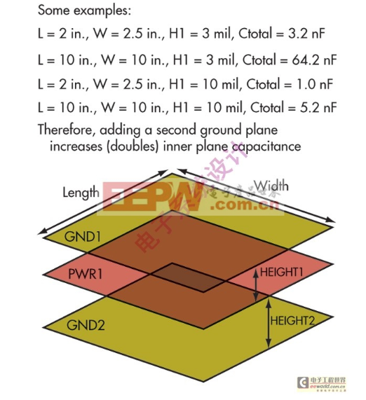
Figure 6: By designing the PCB stack-up with adjacent power and ground planes, high-frequency capacitance can be achieved in the PCB. This will meet lower impedance at higher frequencies.
Minimizing the voltage ripple that occurs in response to power supply current demand is very important for the PDS, but it is often overlooked. All circuits require current, some in large quantities and some at a faster rate. The voltage ripple due to the circuit current demand can be minimized by using a well-decoupled low impedance power or ground plane and a good PCB stackup.
Depending on the decoupling strategy used, if the system is designed to switch current of 1A and the impedance of the PDS is 10mΩ, the maximum voltage ripple is 10mV. The calculation formula is simple: V=IR.
High frequencies can be covered with a perfect PCB stackup, while low frequencies (<500MHz) can be covered with traditional decoupling at the starting entry point of the power plane and around high power or surge current devices. This will ensure that the PDS impedance is the lowest across the entire frequency range.
It is not necessary to place capacitors everywhere, nor is it necessary to break all manufacturing rules to place capacitors right in front of every IC. If such drastic measures are required, there is another problem in the circuit.
Optimizing PCB layout for high-speed ADC design
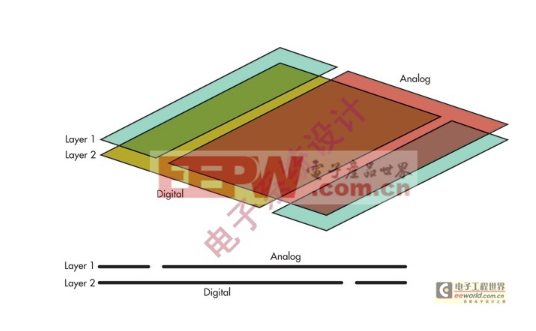
Figure 7: Note: The PCB stackup as a noise layer may be located below, which may couple signals to sensitive analog circuits, layers or planes.
Plane coupling
Some layouts inevitably have overlapping circuit planes (Figure 7). In some cases, there may be a sensitive analog plane (whether it is power, ground or signal) and a noisy digital plane on the next layer. Most designers think this doesn’t matter because the plane is on another layer. So let’s do a simple test.