Overcoming the Challenges of Aligning Multiple Connector Groups Between PCBs
Printed circuit board (PCB) manufacturers face significant pressure to increase density, shrink footprint, reduce side dimensions, manage thermal flow, and increase data rates while improving reliability and reducing costs. As they continue to successfully address these pressures, an interesting challenge has emerged for designers: aligning multiple mated connector groups between two PCBs.
What is needed are clear guidelines to understand how to address these alignment challenges without sacrificing system performance, density, and reliability, while meeting increasingly stringent budget and time-to-market requirements.
This article will discuss the alignment challenges in more detail before describing the conflicting requirements that may be encountered between advanced PCBs and more reliable, high-density connectors, so that these requirements can be efficiently met through the use of design best practices.
Miniaturization makes connector alignment difficult
PCBs have many areas where they can be improved, including density, higher data rates, thermal management, and reliability. However, along with these improvements comes the pressure that the trend toward miniaturization has placed on designers in terms of connector selection and implementation, especially when mating multiple connectors to a PCB.
In the case of connectors, miniaturization over the past 25 years has resulted in pitches dropping from 0.100 inches (2.54 mm) to 0.016 inches (0.40 mm)—a six-fold decrease, necessitating tighter tolerances. Tighter tolerances in themselves are not the problem, however; it’s the variability around the nominal tolerances that is the problem: if multiple connectors are pushed to either extreme of the nominal, then some problems are more likely to occur.
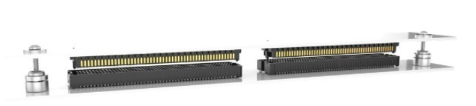
Applications with a single mating connector set will not present a problem: because there is no tolerance stack-up, the mezzanine card is assumed to be free-floating, and the connector’s global and local alignment features will ensure perfect alignment (Figure 1, top).
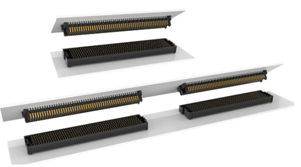
Figure 1: Applications with a single mating connector (top) have no stack-up tolerances, and the connector’s global and local alignment features will ensure perfect alignment. Multiple connectors introduce tolerances that can stack and cause alignment errors. (Image source: Samtec Inc.)
However, adding more mating connector sets in any orientation and at any distance to the same mother mezzanine card will introduce some tolerance stack-up (Figure 2, bottom). These tolerances are particularly important to PCB fabrication shops, electronic manufacturing services, and the properties of the materials used in PCBs.
To illustrate this issue, consider a multi-mezzanine connector system (Figure 2). The assembly includes six or more components: motherboard (A), mezzanine card (B), female connector #1 (C), which mates with male connector #1 (D), and female connector #2 (E) which mates with male connector #2 (F).
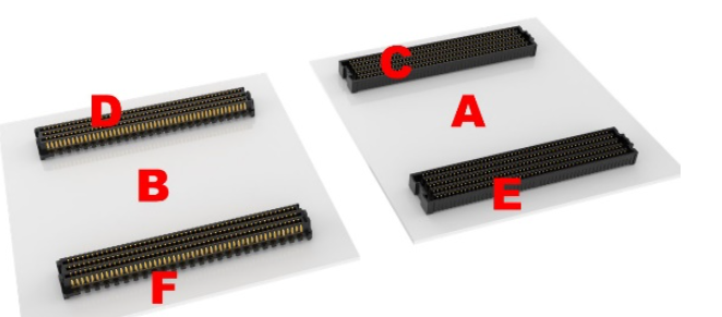
Figure 2: Why designers need to consider and account for the tolerances of all components, including the PCBs.
(Image source: Samtec Inc.)
If the mezzanine connector and sufficiently rigid PCBs were manufactured, processed, and assembled precisely to nominal conditions, an unlimited number of connectors could be successfully deployed between two PCBs; in reality, tolerances and variability in material properties are limiting or determining factors. In the case shown in Figure 2, designers need to consider and account for the tolerances of all components, including the often overlooked but relevant tolerances of the two PCBs (A) and (B).
How to Solve the PCB-to-Connector Alignment Problem
Some PCB procurement projects are controlled only by specifications embedded in Gerber data packets (Figure 3). These data packets can be used to build PCBs without considering mechanical tolerances.
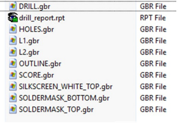
Figure 3: Some PCB procurement projects are controlled only by specifications embedded in Gerber data packets, which can be used to build PCBs without considering mechanical tolerances. For multi-connector applications, this data packet needs to be accompanied by a separate mechanical drawing.
(Image source: Samtec Inc.)
For multi-connector applications, this data packet must be accompanied by a separate mechanical drawing to indicate the artwork, drill and routing tolerances.
At this point, designers need to do two things to help ensure a successful outcome. The first is to understand what support the PCB supplier and connector supplier can provide to ensure alignment. The second is to ensure that system-level tolerance studies have been conducted to determine the connector alignment deviations caused by their design.
Looking back at the multi-connector mezzanine card system composed of components A through F in Figure 2, the connector supplier can only control the tolerances of the connectors. A good supplier will meet or exceed published performance specifications, make PCB board tolerance and processing recommendations, and even provide references to recommended PCB suppliers and equipment as needed.
System or product designers should refer to the connector footprint and product specifications. The misalignment specifications contained in these documents should be compared with the results of system-level tolerance studies to help ensure that multiple connectors between the same boards are used successfully.
As long as the initial and final angular and linear misalignment values are not exceeded, the connector system will function properly. These misalignment values are calculated by considering factors such as insulator interference, beam deflection, and contact friction. Exceeding misalignment values may cause circuit and/or insulator disconnection or damage.
While all the necessary information such as design, component tolerances, equipment, and manufacturing capabilities are usually readily available to designers, it is important to be able to contact the connector manufacturer for more specific guidance and verification of misalignment tolerance stack-up.
Alignment pins are not suitable for multi-connector applications
Some connector manufacturers offer optional alignment pins, which are usually located on opposite sides of the connector bottom (Figure 4). These dowel pins can aid in manual placement and can be used to help orient the connector on the PCB without adding to the overall tolerance stack-up for single-connector applications.
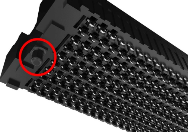
Figure 4: While dowel pins are useful for both manual placement and orientation, they are not recommended for multiple-connector applications because of the impact they can have on the overall tolerance stack-up.
(Image source: Samtec Inc.)
However, dowel pins are not recommended for multiple-connector applications because of the impact they can have on the overall tolerance stack-up. If orientation is still required on the PCB, a better option is to drill oversized holes in the PCB and then machine-place the connector.
Likewise, using jigs or pins to assist in connector placement is not recommended. These methods typically rely on drilling a hole in the PCB relative to the artwork, but the positional tolerance of that hole is often poor, which reduces the overall accuracy of the final placed connector relative to another connector.
For multiple-connector applications, a better approach is to position all pads starting at position A1 in the solder pad array A and then accurately place the connector on the pads before reflow.
Securing the PCB with Captive Screws
Some particularly rugged applications may require the use of captive screws to secure the two PCBs. In this case, the screws should be placed as close to the connector system as possible (Figure 5).
Figure 5: If captive screws are to be used, they should be placed as close to the connector system as possible.
(Image source: Samtec Inc.)
Placing them close together will concentrate stress near the connector and reduce the unsupported PCB span. The increased span induces bending stresses in the PCB, which can adversely affect other components, especially surface-mount components.
Another source of connector-derived PCB stress is the loading process, where a large number of insertions and extractions (I/Os) can generate very large insertion/extraction forces. These forces can cause excessive PCB deflection, requiring additional ribs to support the PCB. It is very important to always confirm the connector insertion and extraction forces, which can be found in the product qualification test report. (Figure 6).
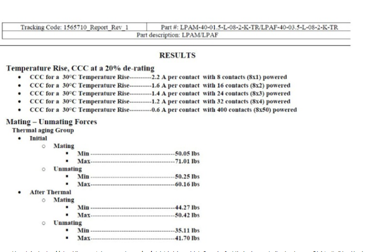
Figure 6: To avoid out-of-spec loading, designers should always confirm the connector insertion and extraction forces, which can be found in the product qualification test report.
(Image source: Samtec Inc.)
Conclusion
Although miniaturization makes it more challenging, it is possible to use multiple connector sets on two PCBs by using best design practices. These include performing a system tolerance study to determine connector alignment deviations, then following the connector provider’s recommended footprint and mold design and utilizing a machine to place the components.
In addition, it is recommended to work closely with the connector provider early in the design process, as they can advise on connector type and placement, and provide consultation on how to minimize overall PCB and connector stress to help ensure a successful design.