Introduction to PCB horizontal electroplating technology
I. Overview
With the rapid development of microelectronics technology, printed circuit board manufacturing has developed rapidly in the direction of multi-layer, stacked, functional and integrated. This has prompted the use of micro-holes, narrow spacing and thin wires in the design of printed circuits for the conception and design of circuit graphics, making the manufacturing technology of printed circuit boards more difficult, especially the aspect ratio of the through holes of multi-layer boards exceeding 5:1 and the deep blind holes used in the stacked boards, so that the conventional vertical electroplating process cannot meet the technical requirements of high-quality and high-reliability interconnection holes.
The main reason needs to be analyzed from the electroplating principle about the current distribution state.
Through actual electroplating, it is found that the distribution of current in the hole is waist-drum-shaped, and the current distribution in the hole gradually decreases from the edge of the hole to the center of the hole, resulting in a large amount of copper deposited on the surface and the edge of the hole. It is impossible to ensure that the copper layer in the center of the hole where copper is needed should reach the standard thickness.
Sometimes the copper layer is extremely thin or there is no copper layer.
In severe cases, it will cause irreparable losses, resulting in a large number of multi-layer boards being scrapped. In order to solve the product quality problem in mass production, the current and additives are currently used to solve the deep hole electroplating problem. In the copper electroplating process of high aspect ratio printed circuit boards, most of them are carried out under relatively low current density conditions with the assistance of high-quality additives, moderate air stirring and cathode movement. The electrode reaction control area in the hole is enlarged, and the effect of the electroplating additive can be shown. In addition, the cathode movement is very conducive to the improvement of the deep plating ability of the plating solution, the polarization degree of the plated parts is increased, and the formation rate of the crystal nucleus and the growth rate of the grains in the electrocrystallization process of the plating layer compensate each other, thereby obtaining a high-toughness copper layer.
However, when the aspect ratio of the through hole continues to increase or deep blind holes appear, these two process measures become powerless, so horizontal electroplating technology is produced. It is a continuation of the development of vertical electroplating technology, that is, a novel electroplating technology developed on the basis of vertical electroplating technology. The key to this technology is to manufacture an adaptive and mutually complementary horizontal electroplating system, which can make the high-dispersion plating solution show better functional effects than the vertical electroplating method with the improvement of the power supply method and other auxiliary devices.
2.Introduction to the Principle of Horizontal Electroplating
The methods and principles of horizontal electroplating and vertical electroplating are the same.
Both must have positive and negative electrodes. After power is applied, an electrode reaction is generated to ionize the main components of the electrolyte, causing the charged positive ions to move to the negative phase of the electrode reaction zone; the charged negative ions move to the positive phase of the electrode reaction zone, thus producing a metal deposition coating and releasing gas.
Because the process of metal deposition at the cathode is divided into three steps: the metal hydrate ions diffuse to the cathode; the second step is that the metal hydrate ions gradually dehydrate when passing through the double electric layer and adsorb on the surface of the cathode; the third step is that the metal ions adsorbed on the cathode surface accept electrons and enter the metal lattice. From the actual observation of the working tank, it is an unobservable heterogeneous electron transfer reaction between the interface of the solid electrode and the liquid electroplating solution.
Its structure can be explained by the double electric layer principle in electroplating theory. When the electrode is the cathode and is in a polarized state, the cations surrounded by water molecules and carrying positive charges are orderly arranged near the cathode due to electrostatic forces. The surface formed by the center point of the cation closest to the cathode is called the Helmholtz outer layer, which is about 1-10 nanometers away from the electrode. However, due to the total amount of positive charge carried by the cations in the Helmholtz outer layer, the positive charge is not enough to neutralize the negative charge on the cathode. The plating solution far from the cathode is affected by convection, and the cation concentration of its solution layer is higher than the anion concentration.
This layer is smaller than the Helmholtz outer layer due to electrostatic forces, and is also affected by thermal motion. The arrangement of cations is not as tight and neat as the Helmholtz outer layer. This layer is called the diffusion layer.
The thickness of the diffusion layer is inversely proportional to the flow rate of the plating solution. That is, the faster the flow rate of the plating solution, the thinner the diffusion layer, and vice versa. The thickness of the diffusion layer is generally about 5-50 microns.
The farther away from the cathode, the plating solution layer reached by convection is called the main plating solution. Because the convection generated by the solution will affect the uniformity of the concentration of the plating solution. The copper ions in the diffusion layer are transported to the outer Helmholtz layer by diffusion and ion migration of the plating solution.
However, the copper ions in the main plating solution are transported to the cathode surface by convection and ion migration. In the horizontal electroplating process, the copper ions in the plating solution are transported to the vicinity of the cathode in three ways to form a double electric layer.
The convection of the plating solution is generated by external and internal mechanical stirring and pump stirring, the swing or rotation of the electrode itself, and the flow of the plating solution caused by temperature difference.
The closer to the surface of the solid electrode, the slower the flow of the plating solution becomes due to the influence of its friction resistance. At this time, the convection rate on the surface of the solid electrode is zero.
The rate gradient layer formed from the electrode surface to the convection plating solution is called the flow interface layer. The thickness of the flow interface layer is about ten times the thickness of the diffusion layer, so the transport of ions in the diffusion layer is almost unaffected by convection.
Under the action of the electric field, the ions in the plating solution are transported by electrostatic force, which is called ion migration. The rate of its migration is expressed by the formula as follows: u = zeoE/6πrη. Among them, u is the ion migration rate, z is the charge number of the ion, eo is the charge of an electron (i.e. 1.61019C), E is the potential, r is the radius of the hydrated ion, and η is the viscosity of the plating solution. According to the calculation of the equation, it can be seen that the greater the potential E drop, the smaller the viscosity of the plating solution, and the faster the rate of ion migration.
According to the theory of electrodeposition, during electroplating, the printed circuit board located on the cathode is a non-ideal polarized electrode. The copper ions adsorbed on the surface of the cathode obtain electrons and are reduced to copper atoms, which reduces the concentration of copper ions near the cathode. Therefore, a copper ion concentration gradient will be formed near the cathode.
The layer of plating solution with a lower copper ion concentration than the main plating solution is the diffusion layer of the plating solution. The copper ion concentration in the main plating solution is higher, and it will diffuse to the place with lower copper ion concentration near the cathode, constantly replenishing the cathode area.
The printed circuit board is similar to a flat cathode, and the relationship between the magnitude of its current and the thickness of the diffusion layer is the COTTRELL equation:
Where I is the current, z is the charge number of the copper ion, F is the Faraday constant, A is the cathode surface area, D is the copper ion diffusion coefficient (D = KT/6πrη), Cb is the copper ion concentration in the main plating solution, Co is the copper ion concentration on the cathode surface, D is the thickness of the diffusion layer, K is the Bozman constant (K = R/N), T is the temperature, r is the radius of the copper hydrate ion, and η is the viscosity of the plating solution. When the copper ion concentration on the cathode surface is zero, its current is called the limiting diffusion current ii:
From the above formula, it can be seen that the magnitude of the limiting diffusion current is determined by the copper ion concentration of the main plating solution, the diffusion coefficient of the copper ion and the thickness of the diffusion layer. When the copper ion concentration in the main plating solution is high, the diffusion coefficient of the copper ion is large, and the thickness of the diffusion layer is thin, the limiting diffusion current is larger.
According to the above formula, to achieve a higher limiting current value, appropriate process measures must be taken, that is, a heating process method must be adopted. Because increasing the temperature can increase the diffusion coefficient, increasing the convection rate can make it eddy current and obtain a thin and uniform diffusion layer. From the above theoretical analysis, increasing the copper ion concentration in the main plating solution, increasing the temperature of the plating solution, and increasing the convection rate can all increase the limiting diffusion current and achieve the purpose of accelerating the plating rate. Horizontal electroplating is based on the formation of eddy currents due to the accelerated convection rate of the plating solution, which can effectively reduce the thickness of the diffusion layer to about 10 microns. Therefore, when using a horizontal electroplating system for electroplating, its current density can be as high as 8A/dm2.
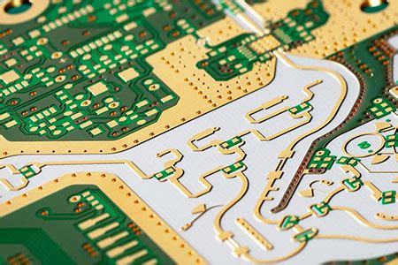
The key to electroplating of printed circuit boards is how to ensure the uniformity of the copper layer thickness on both sides of the substrate and the inner wall of the through hole.
To obtain the uniformity of the plating thickness, it is necessary to ensure that the plating solution flow rate on both sides of the printed circuit board and in the through hole is fast and consistent to obtain a thin and uniform diffusion layer.
To achieve a thin and uniform diffusion layer, from the current structure of the horizontal electroplating system, although many nozzles are installed in the system, the plating solution can be quickly and vertically sprayed to the printed circuit board to accelerate the flow rate of the plating solution in the through hole, resulting in a very fast flow rate of the plating solution, forming eddy currents on the upper and lower sides of the substrate and in the through hole, so that the diffusion layer is reduced and more uniform.
However, usually when the plating solution suddenly flows into a narrow through hole, the plating solution at the entrance of the through hole will also have a reverse reflux phenomenon. Coupled with the influence of the primary current distribution, it often causes the copper layer to be too thick due to the tip effect when the hole is electroplated at the entrance, and the inner wall of the through hole forms a dog-bone-shaped copper plating layer.
According to the state of the plating solution flowing in the through hole, that is, the size of the eddy current and reflux, the state analysis of the quality of the conductive plated through hole can only be determined by the process test method to determine the control parameters to achieve the uniformity of the plating thickness of the printed circuit board. Because the size of the eddy current and reflux cannot be known by theoretical calculation methods, only the actual measurement process method can be used. From the measured results, it is known that in order to control the uniformity of the thickness of the through-hole electroplated copper layer,
it is necessary to adjust the controllable process parameters according to the aspect ratio of the through-hole of the printed circuit board, and even select a copper electroplating solution with high dispersion ability, and then add appropriate additives and improve the power supply method, that is, use reverse pulse current for electroplating to obtain a copper plating layer with high distribution ability.
Especially when the number of micro blind holes in the laminate increases, not only a horizontal electroplating system should be used for electroplating, but also ultrasonic vibration should be used to promote the replacement and circulation of the plating solution in the micro blind holes, and then the power supply method should be improved to use the reverse pulse current and the actual test data to adjust the controllable parameters, and satisfactory results can be obtained.
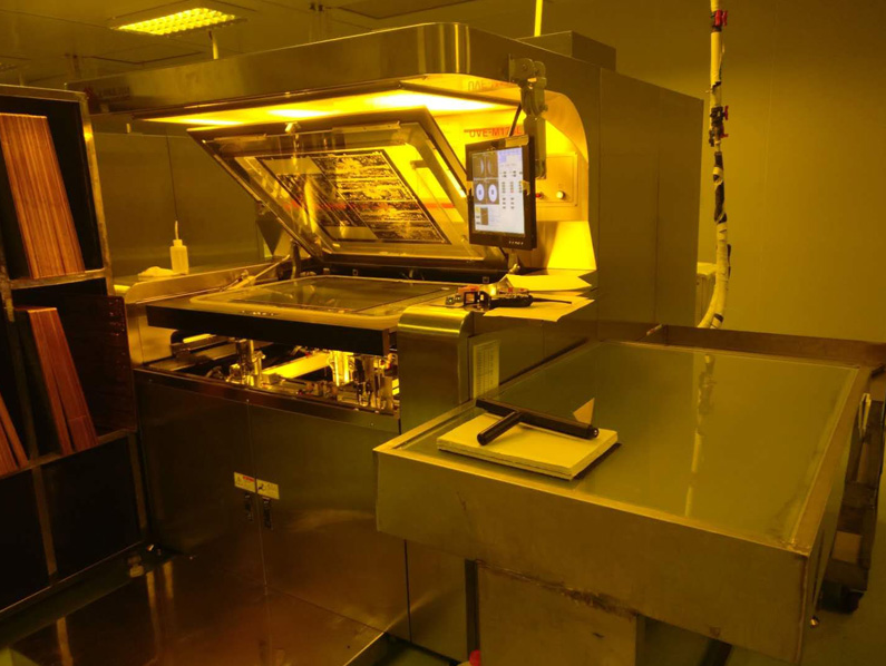
3.Basic structure of horizontal electroplating system
According to the characteristics of horizontal electroplating, it is a plating method that changes the placement of the printed circuit board from vertical to parallel to the surface of the plating solution.
At this time, the printed circuit board is the cathode, and the current supply method of some horizontal electroplating systems uses conductive clips and conductive rollers.
From the convenience of the operating system, the supply method using roller conduction is more common. In addition to being a cathode, the conductive roller in the horizontal electroplating system also has the function of conveying printed circuit boards. Each conductive roller is equipped with a spring device, which is designed to meet the needs of electroplating printed circuit boards of different thicknesses (0.10-5.00mm).
However, during electroplating, the parts in contact with the plating solution may be plated with a copper layer, and the system will not be able to operate over time. Therefore, most of the horizontal electroplating systems currently manufactured are designed to have cathodes that can be switched to anodes, and then use a set of auxiliary cathodes to electrolyze and dissolve the copper on the plated rollers.
For the sake of maintenance or replacement, the new electroplating design also takes into account the easy removal or replacement of parts that are prone to wear. The anode is an insoluble titanium basket with adjustable size, which is placed at the upper and lower positions of the printed circuit board. It contains 25mm diameter spherical copper with a phosphorus content of 0.004-0.006%. The distance between the cathode and the anode is 40mm.
The flow of the plating solution is a system composed of a pump and a nozzle, which makes the plating solution flow rapidly back and forth and up and down in a closed plating tank, and ensures the uniformity of the plating solution flow.
The plating solution is sprayed vertically to the printed circuit board, forming a wall-jet vortex on the surface of the printed circuit board. The ultimate goal is to achieve rapid flow of the plating solution on both sides of the printed circuit board and through holes to form a vortex. In addition, a filtration system is installed in the tank, in which the filter mesh used is 1.2 microns to filter out granular impurities generated during the electroplating process to ensure that the plating solution is clean and pollution-free.
When manufacturing a horizontal electroplating system, it is also necessary to consider the convenience of operation and the automatic control of process parameters. Because in actual electroplating, with the size of the printed circuit board, the size of the through hole aperture, the required copper thickness, the transmission speed, the distance between the printed circuit boards, the size of the pump horsepower, the direction of the nozzle and the current density, the process parameters need to be tested, adjusted and controlled to obtain the copper layer thickness that meets the technical requirements. Computer control is necessary. In order to improve production efficiency and the consistency and reliability of high-end product quality, the through hole pre- and post-processing of the printed circuit board (including plated holes) is carried out according to the process procedures to form a complete horizontal electroplating system to meet the needs of new product development and listing.

4.The development advantages of horizontal electroplating
The development of horizontal electroplating technology is not accidental
, but an inevitable result of the need for special functions of high-density, high-precision, multi-functional, high-aspect ratio multi-layer printed circuit board products. Its advantage is that it is more advanced than the vertical hanging plating process currently used, the product quality is more reliable, and it can achieve large-scale production. Compared with the vertical electroplating process, it has the following advantages:
(1) It can adapt to a wide range of sizes, and does not require manual hanging, and can achieve fully automated operation, which is extremely beneficial to improving and ensuring that the operation process does not damage the substrate surface and realizing large-scale production.
(2) In the process review, there is no need to leave a clamping position, which increases the practical area and greatly saves the loss of raw materials.
(3) Horizontal electroplating adopts full computer control to ensure the uniformity of the surface and hole plating of each printed circuit board under the same conditions.
(4) From the management perspective, the electroplating tank can be fully automated from cleaning to adding and replacing electroplating liquid, and there will be no management out-of-control problems due to human errors.
(5) It can be measured from actual production that since horizontal electroplating adopts multi-stage horizontal cleaning, it greatly saves the amount of cleaning water and reduces the pressure of sewage treatment.
(6) Since the system adopts closed operation, it reduces the pollution of the working space and the direct impact of heat evaporation on the process environment, greatly improving the working environment. Especially when baking the board, the heat loss is reduced, which saves unnecessary energy consumption and greatly improves production efficiency.
5.Summary
The emergence of horizontal electroplating technology is entirely to meet the needs of high aspect ratio through-hole electroplating. However, due to the complexity and particularity of the electroplating process, there are still some technical problems in the design and development of horizontal electroplating systems. This needs to be improved in practice.
Despite this, the use of horizontal electroplating systems is a great development and progress for the printed circuit industry. Because this type of equipment has shown great potential in the manufacture of high-density multi-layer boards, it not only saves manpower and operating time, but also has higher production speed and efficiency than traditional vertical electroplating lines.
It also reduces energy consumption, reduces the waste liquid, waste water and waste gas that need to be treated, and greatly improves the process environment and conditions, and improves the quality level of the electroplating layer. Horizontal electroplating lines are suitable for large-scale production and 24-hour uninterrupted operation. Horizontal electroplating lines are slightly more difficult to debug than vertical electroplating lines. Once debugged, they are very stable. At the same time, during use, the plating solution should be monitored at any time to adjust the plating solution to ensure long-term stable operation.