Why do we need test points on PCB?
For people who study electronics, setting test points on PCB is a natural thing, but for people who study mechanics, what are test points?
Basically, the purpose of setting test points is to test whether the components on the circuit board meet the specifications and solderability. For example, if you want to check whether there is a problem with the resistor on a circuit board, the easiest way is to use a multimeter to measure both ends to find out.
However, in mass production factories, there is no way for you to use an electric meter to slowly measure whether each resistor, capacitor, inductor, or even IC circuit on each board is correct, so the so-called ICT (In-Circuit-Test) automated test machine appeared. It uses multiple probes (generally called “Bed-Of-Nails” fixtures) to contact all the parts circuits on the board that need to be measured at the same time, and then measures the characteristics of these electronic parts in sequence through program control in a sequence-based and parallel-assisted manner. Usually, it only takes about 1 to 2 minutes to test all the parts of a general board, depending on the number of parts on the circuit board. The more parts, the longer the time.
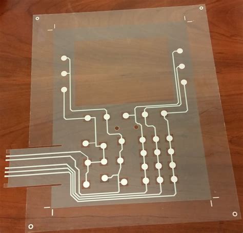
However, if these probes are allowed to directly contact the electronic parts or their solder pins on the board, it is very likely to crush some electronic parts, which is counterproductive. Therefore, smart engineers invented “test points”, which are a pair of round dots at both ends of the parts. There is no solder mask on them, which allows the test probes to contact these dots without directly contacting the electronic parts being measured.
In the early days when traditional plug-ins (DIP) were still used on circuit boards
, the solder pins of parts were indeed used as test points, because the solder pins of traditional parts were strong enough and not afraid of needle piercing, but there were often misjudgments of poor probe contact. Because after general electronic parts are tinned by wave soldering or SMT, a layer of residual film of solder paste flux is usually formed on the surface of the solder. The impedance of this film is very high, which often causes poor probe contact. Therefore, it was often seen that test operators on the production line often used air spray guns to blow desperately, or wiped these places that needed to be tested with alcohol.
In fact, the test points after wave soldering will also have the problem of poor probe contact.
Later, after SMT became popular, the situation of test misjudgment was greatly improved, and the application of test points was also greatly given an important task. Because SMT parts are usually very fragile and cannot withstand the direct contact pressure of the test probe, the use of test points can prevent the probe from directly contacting the parts and their solder pins, which not only protects the parts from damage, but also indirectly greatly improves the reliability of the test, because the misjudgment situation has been reduced.
However, with the development of technology, the size of circuit boards is getting smaller and smaller
. It is already a bit difficult to squeeze so many electronic components on a small circuit board. Therefore, the problem of test points occupying circuit board space is often a tug-of-war between the design end and the manufacturing end. However, this topic will be discussed later. The appearance of the test point is usually round, because the probe is also round, which is easier to produce and easier to make adjacent probes closer, so as to increase the density of needle bed.
- There are some inherent limitations on the mechanism when using a needle bed for circuit testing. For example, the minimum diameter of the probe has a certain limit, and the needle with a too small diameter is easy to break and damage.
- The distance between needles is also limited, because each needle must come out of a hole, and a flat cable must be welded to the back end of each needle. If the adjacent holes are too small, in addition to the problem of contact short circuit between needles, the interference of flat cables is also a big problem.
- Needles cannot be implanted next to some high parts. If the probe is too close to the high parts, there is a risk of collision with the high parts and damage. In addition, because the parts are high, it is usually necessary to open a hole on the test fixture needle bed to avoid it, which indirectly causes the inability to implant the needle. It is becoming increasingly difficult to accommodate the test points of all parts on the circuit board.
- As the boards are getting smaller and smaller, the number of test points has been repeatedly discussed. Now there are some methods to reduce the number of test points, such as Net test, Test Jet, Boundary Scan, JTAG, etc.; there are also other test methods that want to replace the original needle bed test, such as AOI and X-Ray, but at present, each test seems to be unable to replace ICT 100%.
Regarding the implantation capability of ICT, you should ask the cooperating fixture manufacturer, that is, the minimum diameter of the test point and the minimum distance between adjacent test points. Usually there is a desired minimum value and the minimum value that can be achieved by the capability, but large-scale manufacturers will require that the distance between the minimum test point and the minimum test point should not exceed a certain number of points, otherwise the fixture will be easily damaged.