How to control the impedance of the trace during PCB production?
In the field of electronic products, PCB (Printed Circuit Board) is an extremely critical component. Whether it is a high-speed circuit, a high-frequency circuit or a millimeter-wave related product, it is indispensable. The processing of PCB boards is a complex system engineering, covering multiple aspects such as PCB materials, potions, processing technology and line geometry parameters, many of which will affect the impedance of the transmission line.
Factors affecting the impedance of transmission lines
1. Line geometry parameters
(1)Line width
The line width is inversely proportional to the impedance, that is, the wider the line width, the smaller the impedance; the narrower the line width, the greater the impedance. During the production process, if the process is unstable and the line width changes, the impedance will also change accordingly. According to the experience of cooperating with many manufacturers, the change range of the transmission line width is usually around 10%. Set the line width change type to Gauss distribution, set std to 10%, and use ADS CILD for simulation analysis. The results show that the impedance can be as low as 46ohm and as high as 58ohm. On longer transmission lines, this extreme state may cause the return loss to increase and the insertion loss to increase accordingly.
(2)Line length
When the transmission line length increases, the signal transmission path becomes longer, and the distributed capacitance and inductance will also increase accordingly, which will cause the impedance to change. As the line length increases, the signal is affected more complicatedly during the transmission process, and the change in impedance will also have a greater impact on the signal integrity. This is not the characteristic impedance. We simply regard the trace and the reference plane as a capacitance relationship. As the trace becomes longer, the combined capacitance value will also increase.
(3)Line spacing
As the line spacing increases, the coupling capacitance between the lines decreases, and the mutual inductance will also change, which will increase the impedance of the transmission line. Appropriate line spacing is crucial to controlling the impedance of the transmission line and reducing the interference between the lines. When designing PCBs, it is necessary to reasonably set the line spacing according to the specific circuit requirements and signal characteristics.
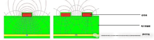
(4)Reference plane
The reference plane is an important factor affecting the impedance of the transmission line in PCB design. The distance between the transmission line and the reference plane, the integrity of the reference plane, and the material of the reference plane will all affect the impedance. When the distance between the transmission line and the reference plane decreases, the capacitance increases and the impedance decreases; conversely, the impedance increases when the distance increases. At the same time, if the reference plane is discontinuous or split, the current distribution of the transmission line will change, thereby changing the impedance. In addition, reference planes of different materials have different conductivity and magnetic permeability, which will also affect the impedance characteristics of the transmission line.
2. PCB material related
(1)Copper foil thickness
In PCB products, copper thickness is divided into base copper thickness and copper plating thickness. Usually the base copper is relatively uniform, but it is not absolute; the uniformity of copper plating varies greatly due to different factory stability. Changes in copper plating thickness will cause changes in transmission line impedance and loss. Assuming that the range of copper plating changes is 10%, statistical analysis is performed through ADS CILD. The results show that the impedance mainly varies between 49.5 and 51ohm, which is smaller than the effect of line width changes on impedance.
(2)Dielectric thickness
During PCB production, changes in dielectric thickness mainly come from raw materials, lamination during production, and glue filling. Once the dielectric thickness changes, it will not only cause impedance changes, but also affect the loss. In severe cases, it may even cause large losses in the transmission line. From the simulation results, the impedance changes are distributed between 44ohm and 54ohm, and the range can reach 10ohm.
(3)Dielectric constant
The dielectric constant has an important influence on the impedance of the transmission line. Generally speaking, the dielectric constant is inversely proportional to the impedance. Different types of PCB boards have different dielectric constants. Even for the same board, its dielectric constant may fluctuate, which in turn affects the impedance of the transmission line.
(4)Dielectric loss angle
The dielectric loss angle also affects the performance of the transmission line.
Put a piece of epoxy printed circuit board material (no copper on both sides) in a microwave oven and heat it at full power for 1 minute. It will be significantly heated by microwaves. Similarly, put a ceramic plate or heat-resistant glass in a microwave oven and it will also be heated. In fact, almost any insulating material can be heated by a microwave oven. The heat absorbed by the insulating material in an alternating electric field environment is proportional to the dielectric loss factor of the material. When insulating materials are used as the insulating medium of transmission lines, dielectric loss will be converted into signal attenuation. The higher the dielectric loss, the greater the attenuation.
If our signal line is attached to a dielectric substrate, the signal is an alternating electromagnetic field with high frequency changes. The effect is the same as putting the substrate in a microwave oven, except that the energy is not as large.
Dielectric loss is a function of frequency. When the frequency of digital devices is lower than 1GHz, the dielectric loss of epoxy resin (FR-4), which is usually used as a printed circuit board material, can be ignored. Under high frequency conditions, the dielectric loss of FR-4 becomes very large. For high-frequency circuits, designers should choose ceramic substrate materials such as alumina. In the case of gigahertz, the dielectric loss coefficient of this type of material is better.
3. Processing technology related
(1)Etching factor
Due to the certain thickness of the conductor, the wire etched during the production process is not a standard “rectangular” structure, but is close to a “trapezoidal” (actually not a complete trapezoid). The angle of the trapezoid changes with the thickness of the copper. The thinner the copper thickness, the closer the angle is to 90°, and the size of this angle will affect the impedance. For example, when the angle is 70°, the impedance is about 50ohm; when the angle is 90°, the impedance is about 48.37ohm.
(2)Etching solution characteristics
The characteristics of the etching solution will affect the etching effect, and then affect the final shape and size of the wire, and indirectly affect the transmission line impedance.
(3)Processing stability
Processing stability is a comprehensive factor that covers multiple links in the production process. Taking the transmission line width as an example, if the process is unstable during PCB production, the line width will change. According to the experience of cooperating with many manufacturers, the variation of the transmission line width is usually around 10%. Set the line width variation type to Gauss distribution, set std to 10%, and use ADS CILD for simulation analysis. The results show that the impedance can be as low as 46ohm and as high as 58ohm. On longer transmission lines, this extreme state may cause the return loss to increase, and the insertion loss will also increase accordingly.
2.Comprehensive Impact Analysis
In the actual production process, the factors that affect the impedance of the transmission line are not a single variable change, but multiple factors may change at the same time. When multiple factors change at the same time, it is found through statistical analysis that the impedance mainly varies between 40ohm and 56ohm, which is far beyond the general requirement of 50±10%. It can be seen that for high-speed and high-frequency circuit products or high-end products, every material, every line geometry parameter and every processing link must be strictly controlled throughout the PCB design and production process, otherwise it is very easy to cause unexpected problems in the product.
The means generally used by PCB factories to adjust the trace impedance are:
When implementing characteristic impedance control, PCB production factories generally use the following methods and processes to ensure that the design meets the signal integrity requirements:
1.Select the appropriate substrate material
Use materials with precise and stable dielectric constants (Dk) and dielectric loss factors (Df), such as FR4, Rogers, PTFE, etc.
Control the thickness of the substrate to ensure the consistency of the distance between layers.
2.Trace width and spacing control
Use impedance calculation tools (such as Polar SI8000, ADS, HyperLynx) to calculate the trace width and spacing according to specific characteristic impedance requirements (such as 50Ω or 100Ω).
Precision PCB production equipment can accurately control the trace width and spacing to the micron level.
3.Stacking structure optimization
Reasonably design the number of layers and interlayer stacking structure of the PCB to ensure that the distance between the signal layer and the reference ground layer meets the impedance requirements.
4.Etching process control
Precisely control the etching time and etching parameters to avoid impedance changes caused by irregular trace width and edges.
Use chemical or laser etching processes to achieve high-precision routing.
5.Pre-compensation design
Considering manufacturing tolerances, appropriately adjust the trace width for pre-compensation during design to ensure that the finished product impedance is close to the design target.
6.Plating thickness control
Control the thickness of the copper layer, because changes in copper thickness will directly affect the characteristic impedance.
Use post-plating etching process or control the thickness of chemical copper plating to ensure consistency.
7.Solder mask thickness and material control
The thickness and dielectric constant of the solder mask will affect the characteristic impedance, so the selection and thickness of the solder mask material need to be strictly controlled.
8.Impedance testing and calibration
During the PCB production process, use an impedance tester (such as a TDR tester) for online or sampling testing.
Adjust production parameters through closed-loop feedback to optimize production results.
9.Differential pair routing control
For differential signals, the routing spacing, routing length difference (skew) and symmetry between differential pairs need to be strictly controlled.