PCB Design to Assembly: Key Steps for Efficient Fabrication
Key Takeaways
Effective PCB assembly begins long before components meet the board. A seamless transition from design to PCBA (Printed Circuit Board Assembly) hinges on meticulous planning, starting with schematic capture and layout optimization. Designers must prioritize manufacturing readiness by adhering to clearance rules, trace-width specifications, and thermal management requirements to prevent fabrication pitfalls like solder bridging or impedance mismatches.
Tip: Always run a Design for Manufacturing (DFM) check before finalizing layouts. This identifies potential assembly conflicts, such as component spacing issues or inadequate copper balancing, which could delay production.
Material selection plays a dual role in PCB development: it impacts both signal integrity and assembly reliability. High-frequency applications demand low-loss substrates like Rogers material, while industrial environments may require high-Tg laminates for thermal stability. Pairing materials with compatible solder masks and surface finishes (e.g., ENIG or HASL) ensures robust connections during PCBA.
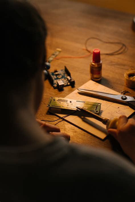
Precision in component placement and reflow soldering separates functional prototypes from mass-production-ready boards. Automated optical inspection (AOI) and X-ray verification are critical for detecting microscopic defects in dense BGA or QFN packages.
Suggestion: Collaborate early with PCBA partners to align design choices with their equipment capabilities. This reduces tooling adjustments and accelerates time-to-market.
Finally, testing protocols validate functionality at every stage—from in-circuit testing (ICT) for individual components to functional testing under real-world conditions. By integrating DFM principles and fostering synergy between design and assembly teams, manufacturers achieve first-pass success while minimizing costly rework.
PCB Design Fundamentals: From Schematic Capture to Layout Optimization
Effective PCB assembly begins with rigorous design practices that bridge conceptual schematics to manufacturable layouts. The process starts with schematic capture, where engineers define electrical connections using tools like OrCAD or Altium Designer. This stage demands meticulous attention to component pinouts, netlist accuracy, and power distribution requirements – errors here cascade into costly PCBA rework during fabrication.
Transitioning to physical layout, designers face critical decisions in component placement and routing strategies. High-speed signals require controlled impedance traces, while power planes must balance current capacity with thermal dissipation. A well-optimized layout minimizes electromagnetic interference (EMI) risks through proper ground plane segmentation and signal path isolation. For PCB assembly efficiency, designers adhere to design for manufacturability (DFM) guidelines, ensuring adequate solder mask clearances and avoiding component shadowing in reflow processes.
Advanced tools now automate design rule checks (DRCs) for trace width compliance and via placement optimization, but human expertise remains vital for resolving conflicting priorities between electrical performance and PCBA feasibility. Layer stack-up configurations must align with both signal integrity needs and the fabrication house’s material capabilities – a mismatch here can derail production timelines. By integrating thermal relief patterns and testability features early in layout phases, teams create designs that transition seamlessly into PCB assembly workflows while meeting IPC-2221 reliability standards.
This foundational work establishes a framework where subsequent stages – from material selection to final testing – build upon verified design parameters, ensuring predictable outcomes in complex electronics manufacturing.
Essential Steps in PCB Development: Ensuring Manufacturing Readiness
Transitioning from design to production requires meticulous attention to manufacturing readiness—a phase where theoretical concepts meet practical execution. The journey begins with design verification, where engineers cross-check schematics against PCB assembly requirements, ensuring component placement aligns with thermal management and signal integrity standards. Critical here is the integration of Design for Manufacturability (DFM) principles, which reduce risks of rework by addressing spacing tolerances, layer stack-up compatibility, and drill-to-copper ratios.
Following design finalization, Gerber file generation and Bill of Materials (BOM) validation form the backbone of fabrication readiness. Missing or mismatched footprints in the BOM can derail PCBA timelines, while incomplete Gerber layers may lead to misinterpretation during board fabrication. Tools like automated DFM analysis software are increasingly deployed to flag potential issues, such as acid traps or insufficient solder mask clearance, before prototypes are ordered.
Another critical phase involves prototyping and testing. Functional prototypes validate not only electrical performance but also mechanical fitment and manufacturability. For instance, surface-mount components requiring precision assembly techniques must undergo thermal stress testing to ensure reliability under operating conditions. Collaboration between design and PCB assembly teams during this stage helps identify process optimizations, such as panelization strategies to maximize yield.
Finally, documentation standardization—including assembly drawings, test protocols, and IPC compliance records—ensures seamless handoff to manufacturing partners. A well-prepared PCBA package minimizes ambiguities, enabling suppliers to replicate designs accurately at scale. By embedding these steps into the development workflow, engineers bridge the gap between innovative designs and repeatable production outcomes.
Material Selection Strategies for High-Performance Circuit Boards
Effective material selection forms the cornerstone of reliable PCB assembly processes, directly impacting thermal stability, signal integrity, and long-term durability. Engineers must balance electrical requirements with mechanical constraints, particularly when designing boards for aerospace, automotive, or IoT applications where extreme temperatures and vibration resistance are critical.
Key Considerations for PCB Materials
| Property | High-Frequency Applications | High-Temperature Environments | Cost-Sensitive Projects |
|---|---|---|---|
| Dielectric Constant (Dk) | ≤3.5 (Rogers RO4000) | ≤4.0 (Polyimide) | ≤4.5 (FR-4) |
| Thermal Conductivity | 0.5-1.5 W/mK | 1.5-3.0 W/mK | 0.3-0.5 W/mK |
| Tg (Glass Transition) | 180°C+ | 200°C+ | 130°C-150°C |
| Cost Multiplier | 5x-8x | 3x-5x | 1x |
For high-speed digital circuits, low-loss laminates like Rogers RO4835™ minimize signal attenuation, while polyimide substrates excel in flexible PCBAs subjected to repeated bending. When optimizing for pcb assembly efficiency, materials with compatible coefficients of thermal expansion (CTE) prevent warping during reflow soldering – a critical factor when using lead-free SAC305 alloys requiring peak temperatures of 245°C.
Recent advancements in halogen-free prepregs address environmental regulations without compromising flame retardancy (UL 94 V-0 rating). For RF/microwave designs, ceramic-filled PTFE composites provide stable Dk values across frequency ranges up to 77 GHz, essential for 5G infrastructure. However, these specialized materials demand precise pcba process controls, including modified etchants and laser ablation parameters.
Material selection directly influences manufacturing yield – boards using Isola IS410’s low-profile copper foil exhibit 18% fewer microvoids in HDI designs compared to standard foils. Always cross-reference material datasheets with your pcb assembly partner’s capabilities, particularly regarding drill hole wall quality and surface finish compatibility (ENIG vs. Immersion Silver).
Precision Assembly Techniques for Reliable Electronics Manufacturing
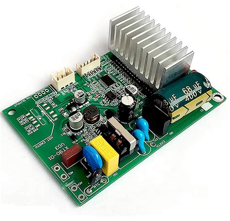
Achieving reliability in electronics manufacturing hinges on meticulous execution during the PCB assembly phase. Modern PCBA (Printed Circuit Board Assembly) processes integrate advanced automation with stringent quality protocols to ensure consistent performance, particularly in mission-critical applications like medical devices or aerospace systems. Central to this phase is surface-mount technology (SMT), which enables high-density component placement through precision pick-and-place machines. These systems, calibrated to micrometer-level accuracy, minimize placement errors while accommodating miniature components such as 01005 resistors or micro-BGA packages.
Reflow soldering follows component placement, requiring precise thermal profiling to avoid defects like tombstoning or cold joints. Optimized temperature curves—tailored to the specific solder paste alloy and component thermal limits—ensure uniform melting and adhesion. For mixed-technology boards combining SMT and through-hole components, selective soldering systems target specific areas, reducing thermal stress on sensitive parts. Post-soldering, automated optical inspection (AOI) and X-ray imaging verify solder joint integrity, flagging issues like bridging or voids that could compromise long-term reliability.
In high-reliability PCBA, conformal coating adds a protective polymer layer to shield circuits from moisture, dust, and chemical exposure. Robotic dispensing systems apply coatings with micron-level consistency, avoiding coverage on connectors or heat sinks. For boards operating in extreme environments, underfill encapsulation reinforces ball grid array (BGA) connections, mitigating mechanical stress from thermal cycling.
Finally, functional testing validates assembly quality through power-up simulations and signal integrity checks. Boundary-scan testing and in-circuit test (ICT) fixtures identify latent faults, ensuring each PCB assembly meets design specifications before integration into end products. By harmonizing these techniques, manufacturers achieve the precision required for today’s complex, miniaturized electronics while maintaining scalability for mass production.
Common Fabrication Pitfalls: How to Avoid Costly Rework
Navigating PCB assembly processes demands meticulous attention to detail, as even minor oversights can escalate into costly delays. One prevalent issue stems from design-for-manufacturability (DFM) oversights, where layout choices conflict with fabrication capabilities. For instance, improperly spaced traces or undersized drill holes may pass design validation but cause etching defects or broken vias during production. To mitigate this, implement DFM checks early, leveraging automated tools to flag clearance violations and thermal imbalances.
Material mismatches represent another critical pitfall. Selecting substrates with incompatible thermal expansion coefficients (TCE) for high-temperature PCBA applications often leads to warping or delamination post-reflow. Partner with fabricators to validate material properties against operational requirements, particularly for multilayer boards or high-frequency designs. Additionally, incomplete documentation—such as missing solder mask specifications or ambiguous layer stackup details—frequently triggers rework cycles. Standardizing Gerber file annotations and including a comprehensive fabrication drawing can resolve 80% of such ambiguities.
Inadequate process controls during PCB assembly further compound risks. For example, improper stencil aperture design for surface-mount technology (SMT) components may result in solder bridging or insufficient joint formation. Adopting statistical process control (SPC) methods to monitor paste deposition accuracy helps maintain consistency across batches. Similarly, neglecting to conduct in-circuit testing (ICT) or automated optical inspection (AOI) before finalizing PCBA units often allows latent defects to reach end-users. Integrating these validation steps at critical milestones reduces failure rates by up to 65%, according to industry benchmarks.
Finally, fostering collaboration between design and fabrication teams remains paramount. Regular cross-functional reviews enable real-time adjustments, ensuring alignment from schematic capture to PCB assembly. By addressing these pitfalls proactively, manufacturers can reduce rework costs by 30–50% while accelerating time-to-market for complex electronics.
Streamlining PCB Workflow: DFM Principles for Quality Production
Implementing Design for Manufacturing (DFM) principles early in the development cycle bridges the gap between theoretical designs and practical production realities. By prioritizing manufacturability during the PCB design phase, engineers can significantly reduce errors, minimize delays, and enhance the reliability of the final PCBA (Printed Circuit Board Assembly). A robust DFM strategy begins with collaboration between design teams and fabrication partners to align technical specifications with production capabilities, ensuring designs adhere to tolerance thresholds and material limitations.
Critical DFM considerations include optimizing component placement for PCB assembly efficiency, maintaining adequate clearances for automated pick-and-place machines, and avoiding high-risk features like ultra-thin traces or insufficient thermal reliefs. For instance, standardized component footprints and land patterns simplify solder mask alignment during PCBA, while unified grid systems streamline drilling and routing processes. Advanced software tools now automate DFM checks, flagging potential issues such as acid traps, starved thermals, or uneven copper distribution that could compromise board integrity.
Material selection plays a pivotal role in DFM execution. Designers must balance thermal conductivity, dielectric strength, and cost efficiency when specifying substrates and finishes. For high-frequency applications, choosing low-loss laminates with consistent dielectric constants ensures signal integrity aligns with fabrication capabilities. Similarly, surface finishes like ENIG (Electroless Nickel Immersion Gold) or HASL (Hot Air Solder Leveling) are evaluated for their compatibility with PCB assembly workflows and end-use environmental conditions.
To further streamline workflows, designers adopt panelization strategies that maximize production yield. Arranging multiple PCBs into a single panel reduces material waste and accelerates mass PCBA processes. However, this requires careful planning of breakaway tabs and scoring lines to prevent damage during depanelization.
By embedding DFM principles throughout the design phase, manufacturers achieve first-pass success rates exceeding 90%, slashing rework costs and accelerating time-to-market. This proactive approach not only refines PCB assembly outcomes but also establishes a repeatable framework for scaling complex electronics manufacturing across industries.
Integrating Design and Assembly: Best Practices for Modern Electronics
Seamless integration between PCB design and pcb assembly processes has become a critical success factor in electronics manufacturing. Cross-functional collaboration between design engineers and PCBA specialists during early development stages ensures design choices align with manufacturing capabilities, reducing costly revisions. Implementing design for manufacturability (DFM) principles—such as optimizing component spacing for automated pick-and-place systems—bridges the gap between schematic concepts and production realities.
A key strategy involves leveraging unified software platforms that synchronize design files with assembly workflows. Tools like automated optical inspection (AOI) compatibility checks and solder mask alignment algorithms preemptively flag conflicts in pad sizing or thermal relief patterns. For high-density boards, prioritizing stackup symmetry and controlled impedance routing minimizes warping risks during reflow soldering—a common pain point in pcb assembly.
Material compatibility remains paramount. Selecting substrates with thermal expansion coefficients matching component packages prevents mechanical stress during PCBA processes. For example, pairing low-loss FR-4 variants with lead-free solder pastes ensures reliable interconnects in high-temperature applications. Additionally, embedding test point accessibility and fiducial marker placement in the layout phase accelerates post-assembly validation.
Advanced manufacturers now adopt model-based enterprise (MBE) frameworks, where 3D PCB models simulate assembly outcomes. This approach identifies collisions between tall components and enclosure features before prototyping. When combined with just-in-time component sourcing databases, it mitigates delays caused by obsolete or mismatched parts during pcb assembly.
To maintain consistency, establish golden rule checks for solder mask clearances, silkscreen legibility, and panelization margins. These standards, when enforced through automated design rule checks (DRC), reduce PCBA defects by up to 62% according to IPC-7351B benchmarks. Finally, instituting closed-loop feedback channels—where assembly technicians report recurring issues to design teams—creates a continuous improvement cycle essential for scaling complex electronics production.
Testing Protocols: Validating PCB Functionality Before Mass Production
Thorough PCB assembly validation ensures reliability and performance before scaling production. Rigorous design verification begins with Design for Testability (DFT) principles, embedding test points and accessibility features into layouts to simplify diagnostics. Automated Optical Inspection (AOI) and In-Circuit Testing (ICT) are critical at this stage, identifying solder defects, component misalignment, or electrical shorts in PCBA prototypes.
Functional testing simulates real-world operating conditions, validating signal integrity, power distribution, and thermal management. For high-density boards, boundary scan testing (IEEE 1149.1) isolates faults in complex interconnects, while environmental stress screening (ESS) exposes weaknesses under temperature cycling or vibration. Statistical process control metrics further refine manufacturing consistency, ensuring each batch meets predefined quality thresholds.
Collaboration between design and PCB assembly teams enhances test coverage. For example, incorporating flying probe testing for small-batch PCBA reduces fixture costs, whereas bed-of-nails fixtures suit high-volume runs. Advanced protocols like burn-in testing for mission-critical applications—such as aerospace or medical devices—prolong stress periods to weed out early-life failures.
Transitioning from prototype validation to mass production requires traceability systems. Barcoding or laser-marked identifiers link test results to specific boards, enabling root-cause analysis for post-production issues. By aligning these protocols with Design for Manufacturing (DFM) guidelines, engineers minimize rework risks and ensure seamless scalability.
Effective testing not only confirms functionality but also quantifies yield rates, providing actionable data to optimize fabrication parameters. This phase bridges PCB assembly outcomes with end-user reliability, solidifying the foundation for consistent, high-quality electronics manufacturing.
Conclusion
The journey from PCB design to functional electronics hinges on seamless integration between engineering creativity and manufacturing precision. While design optimization and material selection set the foundation for performance, the true test of success lies in executing pcb assembly processes with meticulous attention to detail. Modern PCBA workflows demand alignment between design intent and production realities, requiring engineers to anticipate challenges such as component placement accuracy, solder joint reliability, and thermal management.
A critical lesson from industry practice is the value of iterative collaboration between design and manufacturing teams. By implementing design for manufacturability (DFM) principles early, engineers can avoid common pcb assembly setbacks like mismatched pad sizes or inadequate clearance for automated pick-and-place systems. The transition from prototype to mass production becomes significantly smoother when PCBA partners validate designs through pre-production testing, including thermal cycling and in-circuit verification.
Emerging technologies like 3D-printed solder masks and AI-driven inspection systems are redefining quality benchmarks in pcb assembly, enabling faster turnaround without compromising reliability. However, these advancements amplify the need for standardized documentation—from Gerber file annotations to assembly drawings—to prevent interpretation errors during PCBA. As the industry shifts toward high-density interconnects and mixed-material boards, maintaining a holistic view of the entire fabrication chain remains paramount for delivering electronics that balance innovation with durability.
Ultimately, the convergence of robust design practices, material science advancements, and precision pcb assembly techniques forms the backbone of sustainable electronics manufacturing. By treating the PCBA phase not as an endpoint but as a feedback loop for design refinement, teams can achieve both technical excellence and economic efficiency in an increasingly competitive market.
FAQs
How does PCB design impact assembly efficiency?
Effective PCB assembly relies on design-for-manufacturing (DFM) principles. Poorly spaced components or inadequate clearances can complicate PCBA workflows, leading to soldering defects or rework. Optimizing pad sizes, trace widths, and layer stack-ups during design ensures smoother transitions to fabrication.
What materials influence reliability in PCB fabrication?
Thermal stability and signal integrity depend on substrate choices like FR-4, Rogers, or polyimide. For high-frequency applications, low-loss dielectrics minimize interference, while robust copper weights enhance durability. Material selection directly affects PCB assembly yields and long-term performance.
Why is prototyping critical before mass production?
Prototypes validate electrical performance and mechanical fit. Testing at this stage identifies issues like signal crosstalk or thermal stress, reducing costly revisions later. Functional prototypes also help refine PCBA processes, ensuring compatibility with automated pick-and-place systems.
How can designers avoid common fabrication errors?
Adhering to industry standards (IPC-2221, IPC-A-610) prevents issues like acid traps or insufficient annular rings. Clear silkscreen labeling and standardized drill files minimize misinterpretation during PCB assembly. Regular design reviews with fabricators further align expectations.
What distinguishes PCBA from basic PCB fabrication?
PCBA (printed circuit board assembly) integrates components onto the bare board, involving solder paste application, component placement, and reflow soldering. In contrast, fabrication focuses on creating the unpopulated board. Both stages require tight coordination to ensure electrical continuity and mechanical stability.
How does automated testing enhance assembly quality?
Automated optical inspection (AOI) and in-circuit testing (ICT) detect soldering defects, open circuits, or misplaced components. These tools provide quantifiable metrics for PCBA quality, ensuring consistency across production batches and reducing field failure risks.
Optimize Your Next PCB Project Today
Ready to streamline your PCB assembly workflow? Explore advanced PCBA solutions tailored to your design requirements. For expert guidance on fabrication-ready designs, please click here to connect with our engineering team.