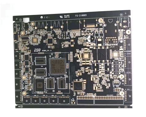
RF PCB Design: A Comprehensive Guide to Optimizing Performance and Reliability
Radio Frequency (RF) circuits are at the heart of modern wireless communication systems, including smartphones, Wi-Fi routers, satellite systems, and radar. Designing RF PCBs (Printed Circuit Boards) is a complex and specialized task that requires careful consideration of signal integrity, impedance matching, electromagnetic interference (EMI), and thermal management. Unlike traditional digital or analog PCBs, RF PCBs operate at high frequencies, where even minor design flaws can lead to significant performance degradation. This article provides a comprehensive guide to RF PCB design, covering key principles, materials, layout techniques, and best practices to ensure optimal performance and reliability.
1. Introduction to RF PCB Design
RF PCBs are designed to handle high-frequency signals, typically ranging from a few megahertz (MHz) to several gigahertz (GHz). At these frequencies, the behavior of electrical signals is significantly different from low-frequency circuits. Factors such as signal reflection, crosstalk, and parasitic capacitance become critical, requiring specialized design techniques and materials. RF PCB design is essential for applications such as wireless communication, radar systems, IoT devices, and medical imaging.
2. Key Principles of RF PCB Design
2.1 Signal Integrity
Signal integrity is the cornerstone of RF PCB design. At high frequencies, signals are more susceptible to losses, reflections, and distortions. Key considerations include:
- Impedance Matching: Ensuring that the characteristic impedance of transmission lines matches the source and load impedances to minimize signal reflections.
- Losses: Minimizing conductor losses (due to trace resistance) and dielectric losses (due to the PCB substrate material).
- Signal Reflections: Avoiding impedance discontinuities, such as sharp bends or vias, which can cause signal reflections.
2.2 Electromagnetic Interference (EMI)
RF circuits are prone to EMI, which can degrade performance and cause interference with other electronic devices. Key strategies to mitigate EMI include:
- Shielding: Using grounded shields or enclosures to block external interference.
- Proper Grounding: Implementing a solid ground plane to reduce ground loops and noise.
- Component Placement: Separating sensitive RF components from noisy digital circuits.
2.3 Thermal Management
RF components, such as power amplifiers, generate significant heat, which must be effectively dissipated to ensure reliability. Key considerations include:
- Thermal Vias: Using thermal vias to transfer heat from components to the ground plane or heat sink.
- Heat Sinks: Integrating heat sinks or cooling systems for high-power components.
- Material Selection: Choosing PCB materials with good thermal conductivity.
3. Materials for RF PCBs
The choice of PCB material is critical for RF applications, as it directly impacts signal integrity, thermal performance, and cost. Common materials include:
3.1 FR-4
FR-4 is a widely used PCB material due to its low cost and good mechanical properties. However, it has relatively high dielectric loss at high frequencies, making it less suitable for RF applications.
- Advantages: Low cost, readily available.
- Disadvantages: High dielectric loss, limited thermal conductivity.
- Applications: Low-frequency RF circuits or cost-sensitive designs.
3.2 Rogers Materials
Rogers Corporation produces specialized high-frequency laminates, such as RO4000 series, which are widely used in RF PCBs.
- Advantages: Low dielectric loss, stable dielectric constant, excellent thermal performance.
- Disadvantages: Higher cost compared to FR-4.
- Applications: High-frequency RF circuits, such as 5G, radar, and satellite systems.
3.3 PTFE (Teflon)
Polytetrafluoroethylene (PTFE) is a high-performance material with excellent electrical properties.
- Advantages: Extremely low dielectric loss, stable dielectric constant.
- Disadvantages: High cost, difficult to process.
- Applications: High-frequency and high-power RF circuits.
3.4 Ceramic-Based Materials
Ceramic materials, such as aluminum oxide (Al₂O₃) and aluminum nitride (AlN), offer superior thermal and electrical properties.
- Advantages: High thermal conductivity, low dielectric loss.
- Disadvantages: Brittle, high cost.
- Applications: High-power RF circuits and harsh environments.
4. RF PCB Layout Techniques
4.1 Transmission Line Design
Transmission lines are used to carry RF signals with minimal loss and reflection. Common types include microstrip, stripline, and coplanar waveguide.
- Microstrip: A trace on the top layer with a ground plane below. Suitable for low to medium frequencies.
- Stripline: A trace sandwiched between two ground planes. Provides better shielding and lower EMI.
- Coplanar Waveguide: A trace with ground planes on the same layer. Offers good impedance control and shielding.
4.2 Impedance Matching
Impedance matching is critical to minimize signal reflections and maximize power transfer. Techniques include:
- Trace Width Calculation: Use impedance calculators to determine the appropriate trace width for the desired impedance (typically 50 ohms for RF systems).
- Matching Networks: Use components such as capacitors and inductors to match impedances at specific frequencies.
4.3 Grounding
Proper grounding is essential to reduce noise and EMI. Key practices include:
- Solid Ground Plane: Use a continuous ground plane to provide a low-impedance return path for RF signals.
- Ground Vias: Place ground vias near RF components to minimize ground inductance.
- Split Ground Planes: Avoid splitting ground planes, as this can create ground loops and increase EMI.
4.4 Component Placement
Component placement plays a crucial role in RF PCB performance. Key guidelines include:
- Minimize Trace Lengths: Place RF components close to each other to minimize trace lengths and reduce losses.
- Separate Analog and Digital Sections: Keep RF and digital circuits physically separated to reduce interference.
- Orientation: Orient components to minimize parasitic capacitance and inductance.
4.5 Via Design
Vias are used to connect different layers of the PCB but can introduce impedance discontinuities and signal reflections. Key considerations include:
- Via Size: Use smaller vias to minimize parasitic capacitance and inductance.
- Via Stubs: Avoid long via stubs by using back-drilling or blind/buried vias.
- Ground Vias: Place ground vias near signal vias to provide a return path and reduce EMI.
5. Simulation and Testing
5.1 Simulation
Simulation tools are essential for validating RF PCB designs before fabrication. Key simulation techniques include:
- Electromagnetic Simulation: Analyze signal integrity, impedance matching, and EMI using tools like ANSYS HFSS or CST Studio Suite.
- Thermal Simulation: Evaluate thermal performance and identify hotspots using tools like FloTHERM or COMSOL.
- Circuit Simulation: Verify the performance of RF circuits using tools like Keysight ADS or NI Multisim.
5.2 Testing
After fabrication, RF PCBs must undergo rigorous testing to ensure performance and reliability. Key tests include:
- Network Analysis: Measure S-parameters to evaluate impedance matching and signal integrity.
- Spectrum Analysis: Analyze the frequency spectrum to detect unwanted signals or harmonics.
- Thermal Testing: Measure temperature distribution to validate thermal management.
6. Applications of RF PCBs
6.1 Wireless Communication
RF PCBs are used in smartphones, Wi-Fi routers, and base stations to enable wireless communication.
6.2 Radar Systems
Radar systems rely on RF PCBs for signal transmission and reception in applications such as aviation, automotive, and defense.
6.3 Satellite Systems
Satellite communication systems use RF PCBs for high-frequency signal processing and transmission.
6.4 Medical Devices
RF PCBs are used in medical imaging systems, such as MRI and ultrasound, for signal processing and data transmission.
7. Emerging Trends in RF PCB Design
7.1 5G Technology
The rollout of 5G networks is driving demand for high-frequency RF PCBs with low loss and high reliability.
7.2 Internet of Things (IoT)
IoT devices require compact, low-power RF PCBs for wireless connectivity.
7.3 Advanced Materials
New materials, such as liquid crystal polymer (LCP) and low-temperature co-fired ceramic (LTCC), are being developed for high-performance RF applications.
7.4 Additive Manufacturing
Additive manufacturing techniques, such as 3D printing, are being explored for prototyping and producing RF PCBs with complex geometries.
8. Conclusion
RF PCB design is a specialized field that requires a deep understanding of high-frequency signal behavior, materials, and layout techniques. By following best practices for signal integrity, EMI mitigation, thermal management, and component placement, designers can create RF PCBs that meet the demanding requirements of modern wireless communication systems. Emerging trends, such as 5G, IoT, and advanced materials, are shaping the future of RF PCB design, offering new opportunities for innovation and performance enhancement. With the right approach, RF PCBs can deliver the reliability and performance needed to power the next generation of electronic devices.