PCB Assembly and Printing Best Practices for Reliable Production
Key Takeaways
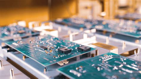
Effective PCB assembly and PCBA processes require a strategic combination of material expertise, precision techniques, and rigorous validation. Durability begins with selecting substrates and laminates that match operational demands, such as high-frequency FR-4 or polyimide for thermal resilience. In precision soldering, controlled reflow profiles and solder paste viscosity are critical to minimizing voids or cold joints. Implementing automated optical inspection (AOI) and X-ray testing ensures defects like tombstoning or bridging are caught early, aligning with quality control protocols.
Optimizing PCB layout involves balancing trace width, spacing, and impedance requirements to reduce signal loss while enhancing manufacturability. Thermal management strategies, including copper pours and via stitching, prevent overheating in high-power designs. Surface finishes like ENIG or HASL not only protect against oxidation but also improve solderability, directly impacting PCB assembly yields. Finally, systematic failure mode analysis for common defects—such as delamination or component misalignment—enables continuous process refinement. By integrating these practices, manufacturers achieve high-yield production with reliable, long-lasting electronics.
PCB Material Selection for Durability
Selecting appropriate materials forms the foundation of durable PCB assembly processes. The choice of substrate, copper weight, and dielectric properties directly impacts a board’s resistance to thermal stress, mechanical strain, and environmental factors. For high-reliability applications, glass transition temperature (Tg) and coefficient of thermal expansion (CTE) become critical parameters—materials like FR-4 with high Tg (≥170°C) or polyimide substrates are preferred for their stability under repeated thermal cycling.
“Always cross-reference material datasheets with your PCBA operating conditions. For instance, aerospace or automotive electronics often require low-loss laminates to minimize signal degradation in harsh environments.”
Copper thickness also plays a pivotal role: heavier copper layers (2–4 oz) enhance current-carrying capacity but require adjustments in pcb assembly soldering profiles to prevent pad lifting. For moisture-sensitive applications, halogen-free or ceramic-filled substrates reduce hygroscopic risks. When combining materials, ensure compatibility between the substrate and surface finishes—immersion silver or ENIG (Electroless Nickel Immersion Gold) are recommended for fine-pitch components to avoid solder joint brittleness. By aligning material properties with end-use requirements, manufacturers can significantly reduce field failures and extend product lifespans.
Precision Soldering for Reliable PCBs
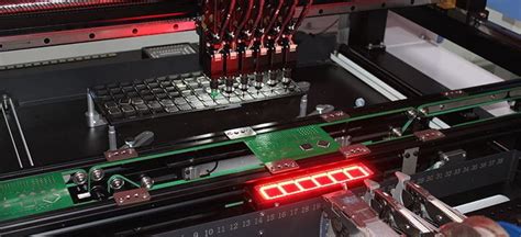
Achieving consistent electrical connectivity in PCB assembly hinges on precision soldering techniques that balance thermal management and material compatibility. Modern PCBA processes prioritize controlled reflow profiles to ensure optimal intermetallic bonding between components and copper pads. For surface-mount devices (SMDs), nitrogen-assisted reflow ovens maintain oxidation-free environments, reducing void formation by up to 60% compared to conventional methods.
Critical to success is the selection of no-clean solder paste with particle sizes matching pad geometries—Type 4 (20-38μm) for fine-pitch ICs and Type 3 (25-45μm) for standard components. Automated optical inspection (AOI) systems now integrate real-time thermal analytics to flag deviations in solder joint formation, enabling immediate adjustments during PCB assembly.
For through-hole components, selective soldering minimizes thermal stress on adjacent SMDs while ensuring barrel fill rates exceed 95%. Engineers increasingly adopt laser-assisted soldering for high-density PCBA designs, achieving micron-level accuracy in heat application. Post-solder cleanliness remains paramount, as ionic contamination below 1.56 μg/cm² (per IPC-5702) prevents electrochemical migration in humid environments.
These methodologies directly influence yield rates in subsequent quality control protocols, forming a foundational layer for defect-free electronics manufacturing.
Quality Control Protocols in PCB Assembly
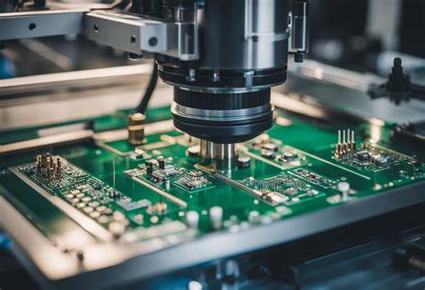
Establishing rigorous quality control protocols in PCB assembly ensures consistent performance and minimizes defects in finished electronics. A multi-stage inspection framework begins with incoming material verification, where substrates, components, and solder pastes undergo compatibility testing against thermal and electrical specifications. During PCBA (printed circuit board assembly), automated optical inspection (AOI) systems scan for misalignments, solder bridging, or insufficient paste deposition, while X-ray imaging validates hidden connections in ball grid arrays (BGAs) or under components.
Post-soldering, functional testing simulates real-world operating conditions to identify intermittent failures or voltage irregularities. Statistical process control (SPC) tools track defect patterns, enabling rapid adjustments to stencil thickness or reflow oven profiles. For high-reliability applications, environmental stress screening (ESS) exposes boards to temperature cycling and vibration to weed out latent flaws.
Critical to these protocols is adherence to IPC-A-610 standards, which define acceptance criteria for solder joint integrity and component placement. Implementing traceability systems with barcoded panels further streamlines root cause analysis, ensuring PCB assembly workflows meet both yield targets and long-term reliability demands.
Optimizing PCB Layout for High Yield
Effective PCB assembly processes begin with intelligent layout design that balances electrical performance and manufacturability. Component placement plays a pivotal role—grouping parts with similar thermal requirements reduces stress during PCBA soldering, while minimizing trace lengths between critical components enhances signal integrity. For high-yield production, adhere to design for manufacturing (DFM) guidelines, such as maintaining adequate clearance between pads (≥0.15mm for fine-pitch components) and avoiding acute angles in trace routing to prevent etching defects.
Prioritize symmetrical copper distribution in multilayer boards to mitigate warpage risks during reflow soldering. Incorporate thermal relief pads for through-hole components to improve heat dissipation and reduce solder joint voids. Additionally, implement testability features like fiducial markers and standardized test points to streamline automated optical inspection (AOI) processes. A well-optimized layout not only reduces PCB assembly errors but also accelerates troubleshooting, directly correlating with higher first-pass yield rates. By aligning design choices with PCBA production capabilities, manufacturers can achieve repeatable precision across large-scale batches.
Thermal Management in PCB Printing
Effective thermal management is critical for ensuring long-term reliability in PCB assembly processes. During printed circuit board fabrication, uneven heat distribution can lead to warping, delamination, or premature component failure. To mitigate these risks, engineers prioritize materials with high thermal conductivity, such as metal-core substrates or ceramics, particularly for high-power PCBA applications.
A key strategy involves optimizing copper weight and trace geometry to balance electrical performance with heat dissipation. Thicker copper layers (2 oz or higher) improve current-carrying capacity while acting as heat spreaders, reducing localized hot spots. For multilayer designs, thermal vias placed beneath power-hungry components—like processors or voltage regulators—channel heat away from sensitive areas, enhancing overall system stability.
In PCB assembly, reflow soldering profiles must align with the substrate’s glass transition temperature (Tg) to prevent board deformation. For example, polyimide-based boards tolerate higher peak temperatures than standard FR-4, making them ideal for aerospace or automotive PCBA where thermal stress is extreme. Post-printing, thermal cycling tests validate the board’s resilience under repeated temperature fluctuations, a protocol mandated in industries like medical device manufacturing.
Proactive thermal design not only extends product lifespan but also minimizes field failures, aligning with quality control objectives outlined earlier in the production workflow.
Surface Finishes Enhancing PCB Performance
The choice of surface finish significantly impacts the reliability, solderability, and long-term performance of PCBA (Printed Circuit Board Assembly). Common finishes like HASL (Hot Air Solder Leveling) provide a cost-effective solution for general-purpose boards, offering robust solder joints for through-hole components. However, for high-density designs requiring finer pitch components, ENIG (Electroless Nickel Immersion Gold) delivers a flatter surface, improving solder pad uniformity and reducing the risk of bridging defects during PCB assembly.
Advanced applications, such as RF or high-speed circuits, often leverage immersion silver or OSP (Organic Solderability Preservative) to minimize signal loss and enhance corrosion resistance. While immersion silver excels in high-frequency performance, OSP is preferred for its environmental compatibility and compatibility with lead-free soldering processes.
Transitioning between finishes requires careful alignment with PCBA requirements. For instance, ENIG’s gold layer ensures excellent oxidation resistance, critical for boards exposed to humid environments, but may increase production costs. Meanwhile, HASL’s thermal resilience makes it ideal for applications involving repeated thermal cycling. Quality validation, including wettability testing and microsection analysis, ensures the selected finish meets both electrical and mechanical demands, directly influencing PCB assembly yield and field reliability.
Troubleshooting Common PCB Assembly Defects
Effective defect resolution in PCB assembly requires systematic analysis and targeted corrective actions. Common issues such as solder bridging, component misalignment, and electrical opens often stem from process inconsistencies or material mismatches. For instance, solder bridges between pins may indicate improper PCBA reflow oven settings, necessitating adjustments to thermal profiling or stencil aperture design.
To streamline troubleshooting, implement a structured approach:
| Defect Type | Root Cause | Corrective Measure |
|---|---|---|
| Solder Bridging | Excessive solder paste deposit | Optimize stencil thickness/aperture design |
| Tombstoning | Uneven component heating | Rebalance reflow oven zones |
| Cold Solder Joints | Insufficient peak temperature | Verify thermocouple calibration |
Advanced diagnostic tools like automated optical inspection (AOI) and X-ray imaging prove invaluable for detecting subsurface flaws in PCB assembly layers. When addressing intermittent connectivity in PCBA units, cross-reference design files with actual layouts to identify potential via fractures or copper trace inconsistencies. Proactive collaboration between design and manufacturing teams reduces defect recurrence by aligning design-for-manufacturability (DFM) principles with process capabilities.
For moisture-related failures in hygroscopic substrates, pre-bake procedures and controlled storage environments mitigate risks. Regularly validate cleaning processes to prevent ionic contamination, particularly in high-frequency PCB assembly applications where residue impacts signal integrity.
Conclusion
Effective PCB assembly and PCBA processes culminate in a holistic approach that integrates material precision, process control, and rigorous testing. While each stage—from thermal management to surface finish optimization—plays a distinct role, their interdependence determines the reliability of the final product. For instance, even the most advanced soldering techniques will underperform if paired with suboptimal layout designs or inadequate quality validation protocols.
To sustain high-yield outcomes, manufacturers must prioritize data-driven adjustments across the production lifecycle. This involves leveraging real-time analytics to refine PCB printing parameters, calibrate assembly workflows, and preemptively address defects. Equally critical is fostering collaboration between design and production teams to align material selection with functional requirements and manufacturability constraints.
As technologies evolve, adopting scalable solutions—such as automation in PCBA or advanced coatings for moisture resistance—ensures adaptability to emerging industry standards. Ultimately, the pursuit of reliability in PCB assembly hinges on balancing innovation with consistency, ensuring every phase reinforces the next in delivering robust, high-performance electronics.
Frequently Asked Questions
What distinguishes PCB assembly from PCBA?
PCB assembly refers to the process of attaching electronic components to a printed circuit board, while PCBA (Printed Circuit Board Assembly) denotes the completed board with all components installed. Both terms are often used interchangeably, but PCBA specifically emphasizes the fully functional end product.
How does material selection impact PCB reliability?
Choosing materials with appropriate thermal stability and dielectric properties ensures resistance to environmental stress. For example, high-Tg laminates prevent warping during PCB assembly, while copper weight selection affects current-carrying capacity.
What are common soldering defects in PCBA?
Frequent issues include cold joints (insufficient heat), bridging (excessive solder), and tombstoning (component misalignment). Implementing reflow profiling and AOI (Automated Optical Inspection) minimizes these defects during PCB assembly.
Why is thermal management critical in PCB printing?
Poor heat dissipation leads to thermal fatigue and premature failure. Techniques like thermal vias, copper pours, and heatsink integration maintain optimal operating temperatures, especially in high-power PCBA applications.
How do surface finishes affect PCB performance?
ENIG (Electroless Nickel Immersion Gold) provides excellent solderability and corrosion resistance, while HASL (Hot Air Solder Leveling) offers cost-effective protection. The choice depends on application requirements and budget constraints in PCB assembly.
Explore Professional PCB Assembly Solutions
For tailored guidance on optimizing your PCB assembly process, please click here to consult our experts at Andwin PCB.