Understanding RPCB Assembly Layers: A Comprehensive Guide to Multilayer PCB Design and Manufacturing
In the realm of modern electronics, multilayer printed circuit boards (PCBs) have become indispensable for achieving high performance, compact designs, and reliable functionality. Among the various types of PCBs, Rigid Printed Circuit Boards (RPCBs) are widely used in applications ranging from consumer electronics to aerospace systems. A critical aspect of RPCB design and assembly is the arrangement and management of layers, which directly impact the board’s electrical performance, thermal management, and manufacturability. This article delves into the concept of RPCB assembly layers, their significance, and best practices for designing and manufacturing multilayer RPCBs.
What Are RPCB Assembly Layers?
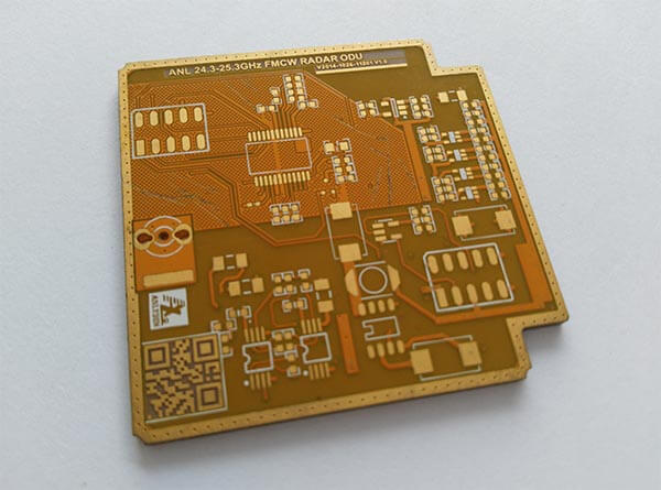
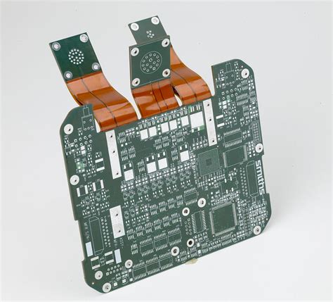
RPCB assembly layers refer to the individual conductive and insulating layers that make up a multilayer rigid PCB. These layers are stacked and bonded together to form a single, cohesive board. Each layer serves a specific purpose, such as signal routing, power distribution, or grounding. The number of layers in an RPCB can vary depending on the complexity of the design, with common configurations ranging from 2 layers to 16 layers or more.
Key Components of RPCB Layers:
- Conductive Layers: These are typically made of copper and are used for signal traces, power planes, and ground planes.
- Insulating Layers: Also known as dielectric layers, these separate the conductive layers and provide electrical insulation. Common materials include FR-4, polyimide, and Rogers laminates.
- Via Layers: Vias are small holes drilled through the PCB to connect different layers. They can be through-hole vias, blind vias, or buried vias.
- Solder Mask Layer: This protective layer covers the conductive traces to prevent short circuits and oxidation.
- Silkscreen Layer: Used for labeling components, test points, and other information.
Importance of RPCB Assembly Layers
The arrangement and management of RPCB assembly layers are crucial for several reasons:
- Signal Integrity:
- Proper layer stacking and routing minimize signal interference, crosstalk, and electromagnetic interference (EMI), ensuring reliable performance in high-frequency applications.
- Power Distribution:
- Dedicated power and ground planes provide stable voltage distribution and reduce noise in the power supply.
- Thermal Management:
- Multilayer RPCBs can incorporate thermal vias and heat-dissipating layers to manage heat generated by high-power components.
- Space Optimization:
- Multilayer designs allow for more compact and lightweight PCBs, which are essential for modern electronics like smartphones and wearables.
- Manufacturability:
- A well-designed layer stackup simplifies the assembly process, reducing the risk of errors and improving yield rates.
Common RPCB Layer Configurations
The choice of layer configuration depends on the complexity of the circuit and the specific requirements of the application. Here are some common configurations:
1. 2-Layer RPCB
- Structure: Top layer (signal) + Bottom layer (signal).
- Applications: Simple circuits, hobbyist projects, and low-cost consumer electronics.
- Advantages: Low cost, easy to manufacture.
- Limitations: Limited routing options, not suitable for high-speed or high-density designs.
2. 4-Layer RPCB
- Structure: Top layer (signal) + Inner layer 1 (ground) + Inner layer 2 (power) + Bottom layer (signal).
- Applications: Moderate complexity designs, such as IoT devices and industrial controls.
- Advantages: Improved signal integrity, better power distribution.
- Limitations: Higher cost than 2-layer boards.
3. 6-Layer RPCB
- Structure: Top layer (signal) + Inner layer 1 (ground) + Inner layer 2 (signal) + Inner layer 3 (power) + Inner layer 4 (signal) + Bottom layer (signal).
- Applications: High-speed digital circuits, automotive electronics, and telecommunications.
- Advantages: Enhanced signal routing, reduced EMI.
- Limitations: Increased complexity and cost.
4. 8-Layer and Above
- Structure: Multiple signal, power, and ground layers arranged in a symmetric or asymmetric stackup.
- Applications: Complex systems like servers, aerospace electronics, and advanced medical devices.
- Advantages: Superior performance, scalability for high-density designs.
- Limitations: High cost, longer lead times.
Designing RPCB Assembly Layers
Designing an effective RPCB layer stackup requires careful planning and consideration of various factors. Here are the key steps and best practices:
1. Define Design Requirements
- Identify the electrical, thermal, and mechanical requirements of the PCB, such as operating frequency, power consumption, and environmental conditions.
2. Choose the Right Materials
- Select dielectric materials based on the application. For example, FR-4 is suitable for general-purpose designs, while Rogers laminates are preferred for high-frequency applications.
3. Plan the Layer Stackup
- Determine the number of layers and their arrangement. A typical stackup includes:
- Signal layers for routing.
- Power and ground planes for stable voltage distribution.
- Symmetric arrangements to minimize warping and improve manufacturability.
4. Optimize Signal Routing
- Use controlled impedance routing for high-speed signals.
- Minimize the length of critical traces to reduce signal loss and delay.
5. Incorporate Thermal Management
- Add thermal vias and heat-dissipating layers to manage heat generated by high-power components.
6. Use Design Tools
- Leverage PCB design software like Altium Designer, KiCad, or Eagle to create and validate the layer stackup.
7. Simulate and Test
- Perform signal integrity and thermal simulations to identify potential issues before fabrication.
Manufacturing RPCB Assembly Layers
The manufacturing process for multilayer RPCBs involves several steps, each requiring precision and expertise:
1. Material Preparation
- Cut and clean the copper-clad laminates and prepreg (pre-impregnated) dielectric layers.
2. Layer Alignment and Bonding
- Align the layers using registration holes and bond them together under heat and pressure.
3. Drilling and Plating
- Drill holes for vias and through-hole components, then plate them with copper to establish electrical connections.
4. Patterning and Etching
- Apply a photoresist layer, expose it to UV light through a mask, and etch away unwanted copper to create the circuit traces.
5. Solder Mask and Silkscreen Application
- Apply the solder mask to protect the traces and the silkscreen for labeling.
6. Testing and Inspection
- Conduct electrical tests, such as continuity and impedance checks, and inspect the board for defects.
Challenges in RPCB Assembly Layers
Designing and manufacturing multilayer RPCBs come with several challenges:
- Signal Integrity Issues:
- High-speed signals can suffer from reflections, crosstalk, and losses if not properly routed.
- Thermal Management:
- High-power components can generate excessive heat, requiring effective thermal vias and heat sinks.
- Manufacturing Complexity:
- Multilayer boards require precise alignment and bonding, increasing the risk of defects.
- Cost and Lead Time:
- Additional layers and advanced materials increase the cost and production time.
- Design Errors:
- Mistakes in the layer stackup or routing can lead to costly rework or failures.
Applications of Multilayer RPCBs
Multilayer RPCBs are used in a wide range of industries and applications, including:
- Consumer Electronics:
- Smartphones, tablets, and laptops rely on multilayer RPCBs for compact and high-performance designs.
- Automotive:
- Advanced driver-assistance systems (ADAS) and infotainment systems use multilayer RPCBs for reliable operation.
- Aerospace and Defense:
- Avionics, radar systems, and satellite communications require multilayer RPCBs for high reliability and performance.
- Medical Devices:
- Imaging systems, pacemakers, and diagnostic equipment use multilayer RPCBs for precision and durability.
- Industrial Automation:
- Control systems, sensors, and robotics rely on multilayer RPCBs for robust and efficient operation.
Conclusion
RPCB assembly layers are a fundamental aspect of modern electronics design and manufacturing. By carefully planning the layer stackup, optimizing signal routing, and addressing thermal and mechanical challenges, engineers can create high-performance, reliable multilayer RPCBs for a wide range of applications.
As technology continues to advance, the demand for multilayer RPCBs will only grow, driven by trends such as 5G, IoT, and autonomous vehicles. By understanding the intricacies of RPCB assembly layers and leveraging best practices in design and manufacturing, engineers can stay ahead of the curve and deliver innovative solutions that meet the evolving needs of the electronics industry. Whether you’re designing a simple prototype or a complex system, mastering the art of RPCB assembly layers is key to achieving success in today’s competitive landscape.