Introduction to 3-Layer PCBs: Design, Applications, and Advantages
Printed Circuit Boards (PCBs) are the backbone of modern electronics, providing a platform for connecting and supporting electronic components. Among the various types of PCBs, the 3-layer PCB is a unique and versatile option that bridges the gap between simple single-layer boards and more complex multi-layer designs. This article explores the design, applications, and advantages of 3-layer PCBs, providing a comprehensive understanding of their role in modern electronics.
What is a 3-Layer PCB?
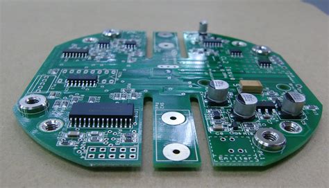
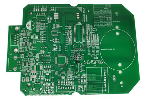
A 3-layer PCB consists of three conductive layers of copper separated by insulating material (typically FR-4). These layers are interconnected through vias, which are small holes drilled into the board and plated with conductive material. The three layers are arranged as follows:
- Top Layer: The outermost layer where most components are mounted. This layer is also used for signal routing.
- Middle Layer: Often used as a ground plane or power plane to provide a stable reference voltage and reduce electromagnetic interference (EMI).
- Bottom Layer: The second outermost layer, typically used for additional signal routing or as a secondary ground/power plane.
The 3-layer PCB is less common than 2-layer or 4-layer boards, as it is often seen as a transitional design. However, it offers specific advantages in certain applications where a balance between complexity and cost is required.
Design Considerations for 3-Layer PCBs
Designing a 3-layer PCB requires careful planning to ensure optimal performance and manufacturability. Below are some key considerations:
1. Layer Stackup
The arrangement of the layers is critical in a 3-layer PCB. A common stackup configuration is:
- Top Layer: Signal routing and component placement.
- Middle Layer: Ground plane for EMI shielding and signal integrity.
- Bottom Layer: Signal routing or power distribution.
The middle layer acts as a reference plane, reducing noise and improving signal quality. Proper stackup design ensures minimal crosstalk and impedance control.
2. Signal Integrity
Signal integrity is a major concern in PCB design. The middle ground plane in a 3-layer PCB helps reduce electromagnetic interference (EMI) and crosstalk between signals. High-speed signals should be routed on the top or bottom layers, with the ground plane providing a return path.
3. Power Distribution
The middle layer can also serve as a power plane, distributing power evenly across the board. This reduces voltage drops and ensures stable operation of components. Decoupling capacitors should be placed near power pins to minimize noise.
4. Thermal Management
Heat dissipation is an important consideration, especially for high-power components. The middle layer can help distribute heat, but additional thermal vias or heatsinks may be required for effective cooling.
5. Manufacturability
3-layer PCBs are more complex to manufacture than 2-layer boards but simpler than 4-layer or higher designs. Designers must ensure that the board can be fabricated within the manufacturer’s capabilities, including minimum trace width, via size, and layer alignment.

Applications of 3-Layer PCBs
3-layer PCBs are used in a variety of applications where a balance between cost and performance is required. Some common applications include:
1. Consumer Electronics
In devices such as smartphones, tablets, and wearables, 3-layer PCBs provide a compact and cost-effective solution for routing signals and managing power distribution.
2. Industrial Control Systems
Industrial equipment often requires robust PCBs that can withstand harsh environments. The middle ground plane in a 3-layer PCB helps reduce EMI, making it suitable for industrial applications.
3. Automotive Electronics
Automotive systems, such as engine control units (ECUs) and infotainment systems, benefit from the EMI shielding and thermal management provided by 3-layer PCBs.
4. Medical Devices
Medical devices require reliable and compact PCBs. The 3-layer design offers a good balance between performance and size, making it ideal for applications such as patient monitoring and diagnostic equipment.
5. LED Lighting
LED drivers and controllers often use 3-layer PCBs to manage power distribution and heat dissipation effectively.
Advantages of 3-Layer PCBs
3-layer PCBs offer several advantages over single-layer and 2-layer designs, making them a popular choice for specific applications. Below are some key benefits:
1. Improved Signal Integrity
The middle ground plane in a 3-layer PCB reduces EMI and crosstalk, ensuring clean signal transmission. This is particularly important for high-speed and high-frequency circuits.
2. Better Power Distribution
Using the middle layer as a power plane ensures even distribution of power across the board, reducing voltage drops and improving the performance of power-hungry components.
3. Compact Design
3-layer PCBs allow for more efficient use of space compared to 2-layer boards, as signals can be routed on both the top and bottom layers. This makes them ideal for compact devices.
4. Cost-Effective
While more expensive than 2-layer PCBs, 3-layer boards are generally more cost-effective than 4-layer or higher designs. They provide a good balance between performance and cost.
5. Thermal Management
The middle layer can help dissipate heat, improving the thermal performance of the board. This is particularly beneficial for high-power applications.
6. Flexibility in Design
Designers have more flexibility in routing signals and distributing power, making it easier to optimize the layout for specific requirements.
Challenges of 3-Layer PCBs
Despite their advantages, 3-layer PCBs also present some challenges:
1. Complexity in Manufacturing
3-layer PCBs are more complex to manufacture than 2-layer boards, requiring precise alignment of layers and careful via placement. This can increase production costs and lead times.
2. Limited Layer Count
For highly complex designs, a 3-layer PCB may not provide enough routing options, necessitating the use of a 4-layer or higher board.
3. Thermal Limitations
While the middle layer can help with heat dissipation, it may not be sufficient for extremely high-power applications. Additional thermal management solutions may be required.
4. Signal Routing Constraints
Designers must carefully plan signal routing to avoid interference and ensure proper impedance matching. This can be more challenging than in 2-layer designs.
Comparison with Other PCB Types
To better understand the role of 3-layer PCBs, it is helpful to compare them with other common PCB types:
1. Single-Layer PCBs
Single-layer PCBs are the simplest and most cost-effective option, but they offer limited routing options and are unsuitable for complex designs.
2. 2-Layer PCBs
2-layer PCBs provide more routing flexibility than single-layer boards but lack the EMI shielding and power distribution capabilities of 3-layer designs.
3. 4-Layer PCBs
4-layer PCBs offer additional layers for signal routing, ground, and power planes, making them suitable for highly complex designs. However, they are more expensive and challenging to manufacture than 3-layer boards.
4. Multi-Layer PCBs
Multi-layer PCBs (6 layers or more) are used in advanced applications such as telecommunications and aerospace. They provide superior performance but come with significantly higher costs and manufacturing complexity.
Future Trends in 3-Layer PCB Technology
As electronics continue to evolve, 3-layer PCBs are likely to play an important role in emerging technologies. Some trends to watch include:
1. Miniaturization
The demand for smaller and more compact devices will drive the use of 3-layer PCBs in applications where space is at a premium.
2. High-Speed Design
With the increasing prevalence of high-speed communication protocols (e.g., 5G, USB 4.0), 3-layer PCBs will need to adapt to meet stringent signal integrity requirements.
3. Advanced Materials
The use of advanced materials, such as high-frequency laminates, will enhance the performance of 3-layer PCBs in high-frequency applications.
4. Sustainability
The electronics industry is increasingly focused on sustainability. Eco-friendly materials and manufacturing processes will become more important in the production of 3-layer PCBs.
Conclusion
3-layer PCBs offer a unique combination of performance, cost-effectiveness, and design flexibility, making them a valuable option for a wide range of applications. While they may not be as common as 2-layer or 4-layer boards, their ability to balance complexity and cost ensures their continued relevance in the electronics industry. By understanding the design considerations, advantages, and challenges of 3-layer PCBs, engineers and designers can make informed decisions when selecting the right PCB for their projects. As technology advances, 3-layer PCBs will continue to evolve, playing a key role in the development of innovative electronic devices.