Printed Circuit Board (PCB) Soldering Defects: Causes, Identification, and Prevention
Introduction
Printed Circuit Boards (PCBs) are the backbone of modern electronics, serving as the platform for interconnecting electronic components. Soldering is a critical process in PCB assembly, as it ensures electrical and mechanical connections between components and the board. However, soldering defects can compromise the functionality, reliability, and longevity of electronic devices. This article explores common PCB soldering defects, their causes, methods for identification, and strategies for prevention.
1. Common PCB Soldering Defects
Soldering defects can occur during manual or automated soldering processes, such as wave soldering, reflow soldering, or hand soldering. Below are some of the most common soldering defects:
1.1. Solder Bridges
Solder bridges occur when excess solder creates an unintended connection between two or more adjacent pins or pads. This can lead to short circuits, malfunctioning circuits, or even component damage.
1.2. Cold Solder Joints
Cold solder joints result from insufficient heat during the soldering process, causing the solder to not fully melt and adhere properly. These joints appear dull, rough, or lumpy and can lead to intermittent connections or complete failure.
1.3. Tombstoning
Tombstoning is a defect where a surface-mount component stands vertically on one of its ends instead of lying flat on the PCB. This occurs due to uneven heating or imbalanced solder paste deposition, leading to poor electrical connections.
1.4. Solder Balling
Solder balling refers to the formation of small spheres of solder that adhere to the PCB or components. These balls can cause short circuits or interfere with the functionality of the board.
1.5. Insufficient Solder
Insufficient solder results in weak or incomplete connections between components and the PCB. This defect can lead to open circuits or unreliable electrical connections.
1.6. Excessive Solder
Excessive solder can create large, bulging solder joints that may interfere with adjacent components or cause short circuits. It can also mask other defects, such as poor wetting.
1.7. Lifted Pads
Lifted pads occur when the copper pad on the PCB separates from the board due to excessive heat or mechanical stress during soldering. This defect can result in open circuits or unstable connections.
1.8. Solder Skips
Solder skips happen when solder fails to adhere to certain pads or joints, leaving them unsoldered. This defect is often caused by poor solder paste application or contamination.
1.9. Voiding
Voids are air pockets or gaps within the solder joint, often caused by trapped flux or moisture during the soldering process. Voids can weaken the mechanical strength of the joint and affect thermal conductivity.
1.10. Component Misalignment
Component misalignment occurs when components are not properly placed on their designated pads before soldering. This can lead to poor electrical connections or mechanical instability.
2. Causes of Soldering Defects
Soldering defects can arise from various factors, including process errors, material issues, and environmental conditions. Below are some common causes:
2.1. Improper Temperature Control
Incorrect soldering temperatures can lead to defects such as cold solder joints, tombstoning, or excessive solder. Too low a temperature prevents proper solder melting, while too high a temperature can damage components or the PCB.
2.2. Poor Solder Paste Quality
Low-quality or expired solder paste can cause issues like solder balling, insufficient solder, or poor wetting. The composition, viscosity, and storage conditions of solder paste play a critical role in soldering quality.
2.3. Contamination
Contaminants such as dust, oil, or oxidation on the PCB or components can prevent proper solder adhesion, leading to defects like solder skips or cold solder joints.
2.4. Incorrect Component Placement
Misaligned or improperly placed components can result in tombstoning, solder bridges, or insufficient solder joints.
2.5. Inadequate Flux Application
Flux is essential for removing oxidation and promoting solder wetting. Insufficient or excessive flux can lead to defects like voiding, solder balling, or poor solder joints.
2.6. Design Flaws
Poor PCB design, such as inadequate pad size, incorrect component spacing, or improper thermal relief, can contribute to soldering defects.
2.7. Equipment Malfunctions
Faulty soldering equipment, such as misaligned stencils, clogged nozzles, or uneven heating, can cause defects like solder bridges, insufficient solder, or tombstoning.
2.8. Environmental Factors
Humidity, temperature fluctuations, and static electricity can affect soldering quality. For example, moisture can lead to voiding, while static discharge can damage sensitive components.
3. Identification of Soldering Defects
Detecting soldering defects early is crucial for ensuring the reliability of electronic devices. Below are some common methods for identifying soldering defects:
3.1. Visual Inspection
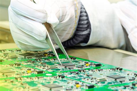
Visual inspection is the simplest and most cost-effective method for identifying soldering defects. Inspectors use magnifying tools or microscopes to examine solder joints for issues like solder bridges, cold joints, or misaligned components.
3.2. Automated Optical Inspection (AOI)
AOI systems use cameras and image processing software to detect soldering defects. These systems can quickly and accurately identify issues like tombstoning, solder balling, or insufficient solder.
3.3. X-Ray Inspection
X-ray inspection is used to detect internal defects, such as voiding or lifted pads, that are not visible to the naked eye. This method is particularly useful for inspecting ball grid array (BGA) components.
3.4. Electrical Testing
Electrical testing, such as in-circuit testing (ICT) or functional testing, can identify soldering defects that affect the electrical performance of the PCB, such as open circuits or short circuits.
3.5. Thermal Imaging
Thermal imaging can reveal defects like cold solder joints or excessive solder by detecting temperature variations across the PCB.
4. Prevention of Soldering Defects
Preventing soldering defects requires a combination of proper process control, material selection, and design considerations. Below are some strategies for minimizing soldering defects:
4.1. Optimize Soldering Parameters
Ensure that soldering temperatures, times, and profiles are optimized for the specific components and PCB materials being used. This can prevent issues like cold solder joints, tombstoning, or excessive solder.
4.2. Use High-Quality Materials
Select high-quality solder paste, flux, and components to minimize the risk of defects. Properly store and handle materials to prevent contamination or degradation.
4.3. Maintain Cleanliness
Keep the PCB and components clean and free from contaminants. Use cleaning agents or plasma treatment to remove oxidation, dust, or oil before soldering.
4.4. Implement Robust Design Practices
Follow best practices for PCB design, such as providing adequate pad size, spacing, and thermal relief. Use design for manufacturability (DFM) principles to ensure compatibility with soldering processes.
4.5. Regular Equipment Maintenance
Regularly inspect and maintain soldering equipment to ensure proper functioning. Calibrate stencils, nozzles, and heating elements to prevent defects caused by equipment malfunctions.
4.6. Train Operators
Provide comprehensive training for operators involved in manual soldering or inspection. Skilled operators are better equipped to identify and prevent soldering defects.
4.7. Control Environmental Conditions
Maintain a controlled environment for soldering, with appropriate humidity and temperature levels. Use anti-static measures to protect sensitive components.
4.8. Conduct Regular Inspections
Implement regular inspections using visual, AOI, or X-ray methods to detect and address soldering defects early in the production process.
Conclusion
Soldering defects can significantly impact the performance and reliability of PCBs, leading to costly rework or product failures. By understanding the common types of soldering defects, their causes, and methods for identification, manufacturers can take proactive steps to prevent these issues. Through optimized processes, high-quality materials, robust design practices, and regular inspections, the occurrence of soldering defects can be minimized, ensuring the production of reliable and high-performing electronic devices.