Essential PCB Production Processes for Modern Electronics
Key Takeaways
When navigating PCB manufacturing, understanding core processes helps you optimize both design and PCB manufacturing cost. You’ll encounter critical stages like substrate preparation, where material selection directly impacts circuit reliability. Modern PCB manufacturing companies rely on advanced etching techniques to achieve micron-level precision, ensuring signal integrity in high-density designs.
Tip: Always verify substrate specifications with your fabrication partner—mismatched materials can lead to costly rework.
For multilayer boards, lamination essentials dictate thermal and mechanical stability. Automated assembly methods, such as pick-and-place systems, streamline production while reducing human error—a priority for scaling your PCB manufacturing business. Surface finish selection balances corrosion resistance and solderability, with options like ENIG or HASL affecting both performance and cost.
Quality testing protocols, including AOI and X-ray inspection, safeguard against defects before final compliance checks. To explore cost optimization strategies further, review industry benchmarks for PCB production. By aligning these steps, you ensure your boards meet technical demands without exceeding budget constraints.
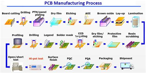
PCB Manufacturing Core Process Breakdown
Understanding the core processes in PCB manufacturing helps you grasp how pcb manufacturing companies transform raw materials into functional circuit boards. It begins with substrate preparation, where fiberglass-reinforced epoxy (FR-4) is laminated with copper to form the base layer. This step directly impacts pcb manufacturing cost, as material quality determines durability and signal integrity.
Next, etching removes excess copper using chemical solutions, leaving precise conductive pathways. Advanced pcb manufacturing business operations employ laser-direct imaging (LDI) for higher accuracy, minimizing waste. Multilayer boards then undergo lamination, bonding inner layers with prepreg resin under heat and pressure—a stage where alignment errors can escalate production expenses.
Automated drilling follows, creating vias for interlayer connections. Here, tooling precision affects both yield rates and long-term reliability. The final stages include plating to reinforce conductive surfaces and solder mask application to prevent short circuits.
Throughout this process, pcb manufacturing companies balance technical complexity with cost-efficiency, often leveraging economies of scale. Whether you’re optimizing pcb manufacturing cost or ensuring compliance, each step in this critical path underscores why meticulous execution defines success in the pcb manufacturing business.
Substrate Preparation for Circuit Reliability
The foundation of reliable PCB manufacturing begins with meticulous substrate preparation, a stage where material selection and surface treatment directly impact circuit performance. You’ll start with a copper-clad laminate, typically FR-4 or polyimide, chosen for its thermal stability and moisture resistance. The substrate undergoes precision cleaning to remove contaminants that could compromise adhesion during etching. For multilayer boards, PCB manufacturing companies often apply specialized treatments—like plasma etching or chemical roughening—to enhance bonding between layers.
Proper substrate preparation minimizes defects such as delamination or conductive failures, which can escalate PCB manufacturing cost due to rework or scrapped batches. Advanced facilities employ laser-drilled alignment markers to ensure layer-to-layer registration accuracy, critical for high-density designs. By prioritizing this phase, you not only improve yield rates but also build a reputation for reliability—a key differentiator in the competitive PCB manufacturing business.
This stage sets the groundwork for subsequent processes, like etching and lamination, where even minor substrate flaws can cascade into functional issues. Investing in quality materials and precision here pays dividends across the entire production lifecycle.
Modern Etching Techniques Explained
When creating printed circuit boards, etching determines the precision of your conductive pathways. Modern PCB manufacturing relies on two primary methods: subtractive etching and additive processes. In subtractive etching, a chemical solution removes excess copper from the substrate, leaving behind the desired circuit pattern. This approach balances PCB manufacturing cost and accuracy, making it a staple for high-volume production. Alternatively, additive techniques build copper traces directly onto the board, reducing material waste—a critical consideration for PCB manufacturing companies aiming to optimize resource efficiency.
Advanced systems now integrate laser direct imaging (LDI), which replaces traditional photomasks with digital patterning. This eliminates alignment errors and supports designs with microscopic tolerances, ensuring consistent performance in complex electronics. However, chemical management remains vital—etchants must be carefully controlled to avoid undercutting traces or damaging the substrate.
For PCB manufacturing businesses, selecting the right etching method hinges on design complexity, volume, and environmental regulations. While subtractive etching suits standardized designs, additive processes excel in prototyping or low-volume runs. Regardless of the technique, modern etching ensures your boards meet today’s demands for miniaturization and signal integrity, seamlessly connecting to subsequent stages like multilayer lamination or automated assembly.
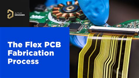
Multilayer Board Lamination Essentials
When building multilayer PCBs, lamination is where precision meets complexity. You start by stacking alternating layers of prepreg (pre-impregnated fiberglass) and copper foil, aligning them with laser-guided systems to ensure micron-level accuracy. PCB manufacturing companies rely on controlled heat and pressure during this phase to bond layers without voids or delamination, which could compromise signal integrity.
The process demands meticulous attention to thermal management—excessive heat warps substrates, while insufficient heat fails to activate the prepreg’s adhesive properties. Modern setups use hydraulic presses with real-time pressure monitoring, balancing PCB manufacturing cost and quality. For high-density designs, sequential lamination might be required, adding steps but enhancing reliability in applications like aerospace or medical devices.
Alignment is equally critical. Misregistered layers create impedance mismatches, leading to signal loss—a costly flaw in high-speed circuits. Advanced PCB manufacturing business operations employ automated optical inspection (AOI) post-lamination to catch alignment errors early.
Finally, curing cycles solidify the bond, with nitrogen-filled chambers preventing oxidation. This step directly impacts the board’s durability, especially in humid environments. By optimizing these variables, you ensure multilayer boards meet performance benchmarks while keeping PCB manufacturing timelines predictable.
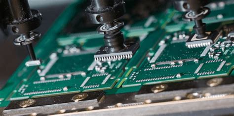
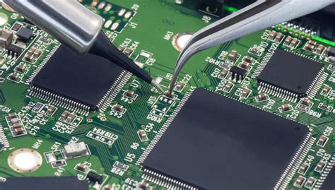
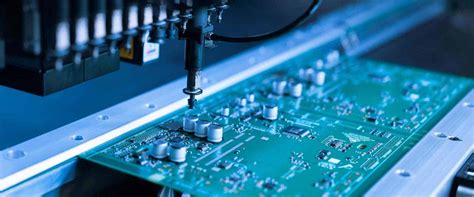
Automated Component Assembly Methods
Automation has revolutionized how PCB manufacturing companies handle component placement, ensuring precision and scalability for high-volume production. Modern assembly lines leverage pick-and-place machines equipped with vision systems to position surface-mount devices (SMDs) with micron-level accuracy. These systems use pre-programmed CAD data to map component locations, reducing human error and accelerating throughput. For through-hole components, automated insertion machines align leads with drilled holes before soldering, maintaining consistency across batches.
A critical advantage of automation lies in controlling PCB manufacturing cost—robotic systems minimize material waste and labor expenses while maximizing yield. Advanced optical inspection (AOI) tools further validate placement accuracy, flagging defects like misalignment or solder bridging in real time. This integration of robotics and quality control ensures that even complex designs, such as multilayer boards, meet stringent reliability standards.
For PCB manufacturing business models targeting rapid prototyping or mass production, automation offers flexibility. Modular systems allow quick reconfiguration for different board sizes or component types, adapting to evolving product demands. By implementing these methods, you not only enhance production efficiency but also strengthen competitiveness in an industry where precision and speed define success.
Surface Finish Selection Criteria
Choosing the right surface finish is critical to ensuring the longevity and performance of your PCB. The finish protects copper traces from oxidation, enhances solderability, and influences signal integrity in high-frequency applications. PCB manufacturing companies prioritize finishes based on end-use requirements, cost constraints, and assembly compatibility.
| Finish Type | Durability | Cost | Common Applications |
|---|---|---|---|
| HASL (Lead-Free) | Moderate | Low | Consumer electronics |
| ENIG | High | Medium | Medical devices, aerospace |
| OSP | Low | Very Low | Prototyping, low-complexity PCBs |
| Immersion Silver | Moderate | Medium | RF/microwave circuits |
When evaluating options, consider how PCB manufacturing cost aligns with your project’s budget. For instance, HASL offers affordability but may struggle with fine-pitch components, while ENIG provides a flat surface for precise soldering—ideal for high-density designs. If you’re managing a PCB manufacturing business, balancing durability and cost becomes pivotal, especially for high-volume orders requiring consistent quality.
Environmental factors also play a role. Lead-free finishes comply with RoHS directives but may require adjustments in soldering profiles. Always collaborate with your PCB manufacturing partner to validate compatibility with your assembly process, ensuring the chosen finish meets both technical and regulatory demands without unnecessary delays.
Quality Testing Protocols Unveiled
After multilayer lamination and component placement, verifying a PCB’s functionality becomes critical. PCB manufacturing companies implement rigorous quality testing protocols to identify defects early, minimizing PCB manufacturing cost escalations from rework or recalls. Automated optical inspection (AOI) systems scan boards for soldering errors, misaligned components, or trace discontinuities—common issues that could compromise performance.
For complex designs, X-ray inspection examines hidden connections in multilayer boards, ensuring internal vias and solder joints meet specifications. Electrical testing follows, where flying probe or bed-of-nails testers simulate operating conditions to detect shorts, opens, or impedance mismatches. These steps are non-negotiable in high-reliability sectors like aerospace or medical devices, where traceability and compliance documentation are mandatory.
Environmental stress tests—such as thermal cycling or humidity exposure—validate durability under extreme conditions. While these protocols add time to the production cycle, they safeguard your PCB manufacturing business reputation by reducing field failures. By balancing thorough testing with lean workflows, you maintain competitiveness without sacrificing quality—a decisive factor when clients evaluate long-term PCB manufacturing partnerships.
Final Inspection and Compliance Standards
Before your PCB reaches its final destination, rigorous final inspection ensures it meets both technical and regulatory benchmarks. This phase combines automated optical inspection (AOI) systems with manual checks to identify microscopic defects like solder bridging or misaligned components. PCB manufacturing companies rely on standards such as IPC-6012 and UL certification to validate performance durability, especially for boards used in aerospace or medical devices.
Compliance isn’t just about functionality—it also addresses environmental and safety regulations. For instance, adherence to RoHS and REACH directives guarantees your PCB manufacturing business avoids hazardous substances, minimizing legal risks. Testing for thermal stress and electrical continuity further ensures reliability under real-world conditions.
Balancing PCB manufacturing cost with quality requires optimizing inspection protocols. Advanced X-ray imaging might escalate expenses but proves critical for multilayer boards. By aligning these checks with client-specific requirements, you maintain competitiveness while delivering boards that exceed industry expectations. Any oversight here could lead to recalls, directly impacting your reputation and partnerships in the electronics supply chain.
Conclusion
As you’ve seen, PCB manufacturing is a tightly coordinated sequence of processes that ensures the reliability and performance of modern electronics. From substrate preparation to final inspection, each step plays a critical role in minimizing defects and maximizing functionality. For PCB manufacturing companies, balancing PCB manufacturing cost with quality demands precision—whether optimizing material usage, refining etching accuracy, or adopting automated assembly systems.
When managing a PCB manufacturing business, understanding these interconnected stages helps you identify efficiency gaps and prioritize investments in advanced technologies. Selecting the right surface finishes or adhering to compliance standards, for example, directly impacts product longevity and client satisfaction. Cost-effective strategies—like bulk material sourcing or predictive maintenance—can further streamline operations without compromising output.
Ultimately, success in this field hinges on aligning technical expertise with strategic planning. By staying informed about evolving fabrication techniques and quality benchmarks, you position your business to meet both current demands and future challenges in electronics production.
Frequently Asked Questions
What factors influence pcb manufacturing cost?
Material selection, board complexity, and order volume primarily determine pcb manufacturing cost. High-density designs or specialized substrates often increase expenses, while bulk orders typically reduce per-unit costs through economies of scale.
How do you choose reliable pcb manufacturing companies?
Evaluate certifications (e.g., ISO, UL), technical capabilities, and client reviews. Reputable pcb manufacturing companies provide design-for-manufacturing (DFM) feedback and transparent timelines, ensuring alignment with your project’s quality and delivery requirements.
What steps ensure consistency in pcb manufacturing?
Automated optical inspection (AOI) and standardized process controls maintain consistency. Advanced pcb manufacturing workflows integrate real-time monitoring systems to detect deviations during etching, lamination, or soldering phases.
Can pcb manufacturing business models adapt to prototyping needs?
Yes, many pcb manufacturing business operators offer flexible services, from low-volume prototyping to mass production. Look for providers with quick-turn options if you require iterative testing before full-scale deployment.
Why are surface finishes critical in final product performance?
Surface finishes like ENIG or HASL prevent oxidation and enhance solderability. Your choice impacts long-term reliability, especially in harsh environments—a key consideration when planning pcb manufacturing strategies.
Ready to Optimize Your PCB Manufacturing Process?
For tailored solutions that balance pcb manufacturing cost and quality, please click here to consult industry experts. Explore advanced techniques tailored to your project’s unique requirements.