Advanced BGA Integration Techniques for PCB Assembly Success
Key Takeaways
Effective PCB assembly processes for BGA (Ball Grid Array) components require a balanced approach combining precision engineering and quality control. Critical considerations include solder paste deposition accuracy and reflow profile optimization, which directly impact PCBA reliability in high-density designs.
"Implementing automated optical inspection (AOI) post-reflow can reduce BGA voiding by 40% compared to manual checks, according to IPC-7095C standards."
Three core pillars define successful integration:
- Thermal management through controlled impedance substrates and thermal relief pads to mitigate stress during thermal cycling
- X-ray inspection for detecting hidden defects like solder bridging or incomplete ball collapse
- Design-for-manufacturing (DFM) principles addressing pad sizing and stencil aperture ratios
For PCB assembly teams, maintaining component moisture sensitivity level (MSL) compliance and using nitrogen-assisted reflow environments prove essential for minimizing oxidation in fine-pitch BGAs. When executed systematically, these strategies enhance PCBA yield rates while meeting J-STD-001 Class 3 requirements for mission-critical applications.
Optimizing BGA Integration in PCB Assembly
Achieving reliable BGA integration in PCB assembly demands meticulous attention to design, material selection, and process control. Modern PCBA workflows prioritize pad geometry optimization and solder mask alignment to accommodate the fine pitch and high I/O density of BGA packages. A critical factor lies in balancing reflow soldering profiles—ensuring sufficient thermal energy for solder joint formation while preventing warpage or voiding.
| Parameter | Traditional Approach | Advanced Optimization |
|---|---|---|
| Reflow Peak Temperature | 240–245°C | 230–235°C (low-void alloys) |
| Solder Paste Type | SAC305 | High-Reliability SAC-Q |
| Placement Accuracy | ±25 μm | ±10 μm (laser-guided) |
Incorporating thermal relief vias and copper balancing techniques mitigates uneven heat distribution during assembly, a common cause of BGA solder joint failures. For high-density PCB designs, staggered ball arrangements and optimized pad sizes reduce bridging risks. Post-solder inspection combines automated optical inspection (AOI) with X-ray imaging to validate joint integrity beneath the package.
To enhance PCBA yield, manufacturers employ predictive modeling to simulate thermal expansion mismatches and refine stencil designs for precise paste deposition. Proactive process validation—such as solder paste volume verification—ensures consistent results across batches. By integrating these strategies, PCB assembly teams can address the unique challenges of BGA integration while maintaining scalability for complex, miniaturized electronics.
Precision Soldering for Reliable BGA Connections
Achieving robust electrical and mechanical bonds in BGA (Ball Grid Array) components demands meticulous control over soldering parameters during PCB assembly. Modern reflow soldering processes utilize precisely calibrated thermal profiles to ensure uniform melting of solder balls while preventing thermal stress on delicate substrates. Critical factors include maintaining optimal peak temperatures (typically 230–250°C) and controlled ramp rates to avoid voiding or cold joints that compromise connectivity.
Advanced PCBA workflows now integrate nitrogen-assisted reflow environments to minimize oxidation, enhancing solder wetting for finer-pitch BGAs. Laser soldering systems further address challenges in high-density layouts by targeting specific joints with micron-level accuracy, particularly useful for mixed-technology boards. Proper solder paste selection—balancing alloy composition (e.g., SAC305) and particle size—ensures consistent volume deposition, critical for bridging gaps between BGA pads and PCB lands.
Post-soldering, automated optical inspection (AOI) and X-ray imaging verify joint integrity, detecting hidden defects like head-in-pillow formations. These techniques, combined with statistical process control (SPC), enable real-time adjustments to soldering parameters, aligning with broader goals of high-density PCB performance and manufacturing yield optimization. By refining these precision techniques, manufacturers mitigate risks of field failures while supporting the miniaturization trends driving modern electronics.
Thermal Management Strategies for BGA Reliability
Effective thermal management remains critical for maintaining BGA reliability in modern PCB assembly processes. As component densities increase in PCBA designs, managing heat dissipation becomes paramount to prevent solder joint fatigue, delamination, and premature device failure. Engineers employ thermal vias beneath BGA packages to create conductive pathways, channeling heat away from sensitive components. Pairing these with optimized thermal interface materials (TIMs)—such as high-performance thermal pads or epoxy-based adhesives—enhances heat transfer to heat sinks or board layers.
For high-power applications, copper-filled vias and strategically placed thermal relief pads balance temperature distribution while minimizing mechanical stress during thermal cycling. Advanced PCBA workflows integrate simulation tools like finite element analysis (FEA) to predict hotspot formation and validate cooling solutions before prototyping. Additionally, selecting substrates with low thermal expansion coefficients (CTE) ensures compatibility with BGA solder balls, reducing warpage risks during reflow soldering.
Proactive monitoring of reflow profiles further safeguards against thermal shock, with ramp rates and peak temperatures calibrated to the specific BGA alloy composition. Combining these strategies with post-assembly infrared thermography enables manufacturers to verify thermal performance and align outcomes with reliability benchmarks for high-density electronics.
Advanced Inspection Methods for BGA Quality
Ensuring the integrity of BGA (Ball Grid Array) components in PCB assembly requires specialized inspection techniques tailored to high-density designs. Non-destructive testing methods, such as 3D X-ray imaging, enable manufacturers to scrutinize solder joints beneath the BGA package, detecting voids, misalignment, or bridging that could compromise electrical connectivity. Automated Optical Inspection (AOI) systems complement this by analyzing surface-level defects, including solder ball coplanarity and pad contamination, which are critical for maintaining PCBA reliability.
For mission-critical applications, electrical testing combined with thermal cycling validates long-term performance under operational stresses. Advanced systems now integrate machine learning algorithms to classify defects with over 99% accuracy, reducing false positives and accelerating troubleshooting. Real-time process feedback from these tools also allows PCB assembly teams to refine solder paste deposition and reflow profiles, directly enhancing manufacturing yield.
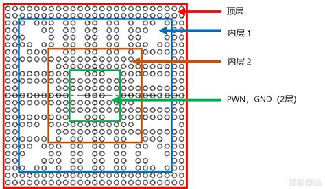
As BGA pitches shrink below 0.3mm, high-magnification microscopy and cross-sectional analysis become indispensable for verifying microvoid distribution and intermetallic compound formation. By layering these inspection strategies, PCBA providers can preemptively address latent defects, ensuring robust BGA integration while aligning with the escalating demands of miniaturized electronics.
Ensuring High-Density PCB Performance With BGA
Achieving optimal performance in high-density PCB assembly requires meticulous attention to BGA (Ball Grid Array) integration, particularly as modern electronics demand smaller footprints and higher functionality. Signal integrity and thermal dissipation become critical challenges when packing hundreds of interconnected components into compact PCBA designs. By leveraging advanced substrate materials like low-loss laminates and optimizing via-in-pad structures, engineers can mitigate impedance mismatches and reduce crosstalk in densely routed boards.
To ensure reliable BGA performance, precise control over solder joint geometry is essential. This involves selecting solder alloys with coefficients of thermal expansion (CTE) that closely match those of the PCB and BGA components, minimizing stress during thermal cycling. Additionally, implementing embedded trace substrates or microvia technologies helps shorten signal paths, enhancing electrical performance while maintaining mechanical stability.
Automated optical inspection (AOI) and X-ray imaging play pivotal roles in validating BGA alignment and solder quality, especially in high-density configurations where visual access is limited. Pairing these techniques with real-time thermal profiling during PCBA reflow ensures consistent solder joint formation, reducing the risk of voids or cold joints. By integrating these strategies, manufacturers can balance miniaturization demands with the stringent reliability requirements of advanced electronics.
Maximizing Yield in BGA PCB Manufacturing
Achieving high manufacturing yields in PCB assembly processes involving BGA components requires meticulous attention to process controls, material selection, and inspection protocols. Statistical process control (SPC) systems play a critical role in monitoring variables such as solder paste deposition accuracy and reflow oven temperature profiles, which directly impact PCBA reliability. Implementing closed-loop feedback mechanisms between stencil printing and post-reflow inspection stages helps identify deviations early, reducing scrap rates by up to 30% in high-volume production.
Material compatibility is equally vital—selecting BGA substrates with coefficient of thermal expansion (CTE) values that align with the PCB base material minimizes stress-induced failures during thermal cycling. Advanced solder alloys with reduced voiding tendencies further enhance joint integrity, particularly in applications requiring extended thermal cycling performance. For PCB assembly teams, integrating automated optical inspection (AOI) and 3D X-ray systems ensures comprehensive defect detection, from solder ball bridging to subsurface microcracks that traditional methods might miss.
To sustain yield improvements, manufacturers must prioritize process documentation and operator training, particularly for handling fine-pitch BGAs below 0.4mm pitch. Establishing golden sample benchmarks for acceptable void percentages (typically <15%) and shear strength thresholds creates clear quality targets. By combining these strategies with real-time data analytics, PCBA providers can systematically address yield-limiting factors while maintaining compatibility with subsequent sections on thermal management and inspection methodologies.

BGA Rework Techniques for Enhanced Assembly Success
Effective BGA rework is critical in PCB assembly processes to address defects without compromising board integrity. Modern high-density designs demand precise methodologies for removing and replacing Ball Grid Array components, particularly when addressing solder joint failures or component misalignment. A systematic approach begins with localized preheating to minimize thermal stress on adjacent components, followed by targeted heating using infrared or hot-air systems to melt solder balls uniformly. Advanced PCBA workflows incorporate vacuum-assisted removal tools to extract faulty BGAs cleanly, reducing the risk of pad damage.
Post-removal, surface preparation ensures optimal adhesion for new components. Applying low-voiding solder paste and controlled reflow profiles (with ramp rates under 3°C/sec) helps achieve reliable interconnects. Real-time monitoring via thermocouples prevents overheating, while post-reflow inspections using 3D X-ray imaging or automated optical inspection (AOI) verify joint integrity and alignment. For complex multilayer boards, sequential rework protocols maintain structural stability by limiting repeated thermal cycles.
Proactive defect mitigation also involves validating rework outcomes through electrical testing and thermal cycling simulations. By integrating these techniques into PCB assembly lines, manufacturers reduce scrap rates and enhance yield, particularly in applications requiring fine-pitch BGAs. Proper tool calibration and operator training remain pivotal to ensuring consistent results across PCBA production batches.
Proactive Defect Prevention in BGA PCB Processes
Effective PCB assembly of BGA components demands rigorous defect prevention strategies to mitigate risks in high-density designs. By integrating design-for-manufacturing (DFM) principles early, engineers can address potential issues such as pad alignment errors or insufficient solder mask clearance. Implementing automated optical inspection (AOI) during PCBA stages enables real-time detection of solder ball bridging or voids, reducing post-assembly rework.
Thermal profiling plays a critical role in preventing defects like warping or delamination. Precise control of reflow oven parameters ensures uniform heat distribution across BGA substrates, minimizing stress on interconnects. Pairing this with moisture-sensitive component handling protocols prevents popcorn effects during reflow, particularly for fine-pitch packages.
Material selection further enhances reliability. Using high-quality PCB assembly materials, such as low-voiding solder pastes and thermally stable substrates, improves BGA solder joint integrity. Additionally, predictive analytics tools analyze historical process data to identify failure patterns, enabling proactive adjustments in PCBA workflows.
By combining advanced inspection technologies, optimized thermal management, and data-driven process refinements, manufacturers can systematically reduce defect rates while maintaining alignment with broader goals of high-density PCB performance and yield optimization.
Conclusion
Effective PCB assembly processes demand meticulous attention to BGA integration, where precision and technical expertise converge to achieve high-performance outcomes. By prioritizing precision soldering methods, implementing robust thermal management protocols, and leveraging advanced inspection technologies, manufacturers can significantly enhance the reliability of BGA-enabled PCBA designs. These strategies not only address the challenges of high-density circuit boards but also align with the industry’s growing emphasis on yield optimization and defect prevention.
As PCB assembly evolves, the interplay between material selection, process automation, and quality validation remains critical. Manufacturers must adopt a proactive approach to defect mitigation, ensuring that BGA rework and process adjustments are guided by data-driven insights. Ultimately, the success of PCBA projects hinges on balancing technical innovation with stringent quality standards, fostering both performance consistency and long-term product durability. By integrating these principles, stakeholders can confidently navigate the complexities of modern electronics manufacturing while maintaining competitiveness in an increasingly demanding market.

Frequently Asked Questions
What are the primary challenges in BGA integration during PCB assembly?
Achieving reliable BGA connections requires overcoming solder joint visibility issues and managing thermal expansion mismatches. Advanced PCBA processes employ X-ray inspection and controlled reflow profiles to address these challenges while maintaining high-density circuit integrity.
How does thermal management impact BGA reliability?
Excessive heat can cause solder joint fatigue or delamination. Effective strategies combine thermal vias, heatsinks, and material selection to dissipate heat efficiently, ensuring BGA-based boards meet performance benchmarks in demanding applications.
Which inspection methods ensure quality in PCB assembly with BGAs?
Automated optical inspection (AOI) and 3D X-ray imaging detect hidden defects like voids or misalignments. These methods complement electrical testing to verify BGA functionality before finalizing PCBA workflows.
Can BGAs be reworked if defects are identified post-assembly?
Yes, specialized tools such as hot-air rework stations enable precise solder ball replacement. However, success depends on maintaining reflow temperature consistency and avoiding collateral damage to adjacent components.
How do manufacturers optimize yield in high-density PCB assembly?
Process controls like solder paste stencil optimization and moisture-sensitive component handling reduce defects. Real-time monitoring during PCBA stages further minimizes rework, aligning with six-sigma manufacturing principles.
Ready to Elevate Your BGA Integration Strategy?
For expert guidance on implementing these solutions in your next project, please click here. Our team specializes in advanced PCB assembly techniques tailored for BGA-driven designs, ensuring manufacturability and performance excellence.