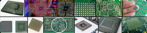
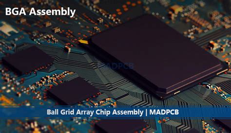
BGA PCB Assembly: Optimizing Precision for Reliable Electronics

Key Takeaways
Effective BGA PCB assembly relies on meticulous attention to precision, thermal dynamics, and quality assurance. Central to this process is precision soldering, which ensures proper electrical connectivity for BGA components through controlled reflow profiles and advanced ball grid array alignment techniques. Rigorous quality control methods, including automated optical inspection (AOI) and X-ray verification, are critical to detecting voids, misalignments, or solder bridging in PCBA workflows.
Thermal management remains a cornerstone of reliability, with optimized heat dissipation strategies—such as thermal vias, heatsinks, and substrate material selection—preventing overheating in high-density layouts. Below is a comparative overview of thermal solutions:
| Thermal Solution | Application | Impact on Reliability |
|---|---|---|
| Thermal Vias | High-power BGA designs | Enhances heat transfer to inner layers |
| Heatsinks | Consumer electronics | Reduces component junction temps by 15–25% |
| Ceramic Substrates | Automotive/Industrial systems | Improves thermal stability under extreme conditions |
Adopting best practices—such as solder paste stencil optimization and nitrogen-assisted reflow—ensures consistent PCB assembly outcomes. Advanced techniques like 3D SPI (Solder Paste Inspection) further refine defect detection, aligning with the demand for miniaturized, high-performance electronics. By integrating these strategies, manufacturers achieve reliable electronics that meet stringent industry standards while balancing cost and complexity in BGA PCB assembly.
Precision Soldering for BGA PCBs
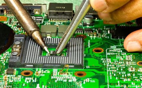
Achieving reliable PCB assembly for Ball Grid Array (BGA) components demands meticulous attention to soldering precision. Unlike traditional packages, BGAs feature hidden solder joints beneath the component, making visual inspection impractical. This necessitates advanced techniques such as controlled reflow soldering and laser-aligned placement systems to ensure uniform solder ball formation.
Tip: Use solder paste stencils with laser-cut apertures to maintain consistent volume deposition, critical for minimizing voids and bridging in PCBA processes.
Modern PCB assembly workflows integrate automated optical inspection (AOI) and X-ray imaging to validate joint integrity post-reflow. X-ray systems, in particular, enable non-destructive analysis of subsurface connections, detecting micro-cracks or misalignments invisible to conventional methods. For high-density designs, thermocompression bonding further enhances joint reliability by applying precise heat and pressure to each connection.
"Even minor deviations in temperature profiles can compromise BGA solder joints. Always calibrate reflow ovens to match the thermal mass of the assembly."
Material selection also plays a pivotal role. High-quality solder alloys with low voiding rates, combined with nitrogen-enriched reflow environments, reduce oxidation risks. By prioritizing these factors, manufacturers ensure PCBA outcomes meet the stringent demands of aerospace, medical, and automotive applications where failure is not an option.
BGA Assembly Quality Control Methods
Effective BGA PCB assembly demands rigorous quality control protocols to ensure long-term reliability in high-performance electronics. Central to this process is the implementation of automated optical inspection (AOI) systems, which detect solder joint defects like voids or bridging with micron-level precision. For PCBA involving ball grid arrays, X-ray inspection becomes indispensable, enabling technicians to visualize subsurface connections and verify proper alignment of hidden solder balls.
Thermal profiling during reflow soldering is another critical checkpoint, as uneven heating can lead to cold joints or warping. Advanced PCB assembly facilities employ real-time monitoring systems to maintain optimal temperature gradients, ensuring consistent solder reflow across the entire BGA footprint. Post-assembly, boundary scan testing validates electrical connectivity, while environmental stress screening (ESS) subjects components to thermal cycling and vibration to simulate real-world operating conditions.
To maintain traceability, manufacturers integrate serialized data tracking throughout the PCBA workflow, linking each BGA to its specific process parameters. This approach not only streamlines defect root-cause analysis but also supports compliance with industry standards like IPC-7095 for BGA implementation. By combining these methodologies, engineers achieve defect rates below 50ppm in mission-critical applications, balancing precision with scalable production demands.
Thermal Management in BGA Assembly
Effective thermal management in BGA PCB assembly is critical for ensuring long-term reliability in high-performance electronics. As ball grid array (BGA) components generate significant heat during operation, PCBA designs must incorporate strategies to dissipate thermal energy without compromising structural integrity. This begins with selecting substrates with optimal thermal conductivity, such as metal-core or ceramic-based materials, which reduce hotspots in densely packed circuits.
Advanced PCB assembly processes employ underfill materials to reinforce solder joints and mitigate thermal stress caused by repeated expansion and contraction. Additionally, precision-controlled reflow soldering profiles ensure uniform heat distribution during component placement, minimizing void formation in solder connections. Engineers often integrate thermal vias and copper planes into the board layout to enhance heat transfer away from critical components.
For applications requiring extreme thermal stability, PCBA manufacturers may implement phase-change materials (PCMs) or active cooling solutions like micro-heat sinks. Rigorous thermal cycling tests validate designs under simulated operating conditions, ensuring compliance with industry standards such as IPC-7095D. By balancing material selection, layout optimization, and process control, BGA assembly achieves the thermal resilience necessary for aerospace, automotive, and IoT devices where failure is not an option.
Reliable Electronics via BGA Optimization
Achieving reliability in modern electronics demands meticulous optimization of BGA (Ball Grid Array) components during PCB assembly. These packages, known for their high-density interconnects, require precise alignment and controlled reflow processes to ensure robust solder joint formation. Thermal stress management plays a critical role here, as uneven heat distribution during PCBA can lead to microcracks or voids, compromising long-term performance. Advanced manufacturers employ design-for-manufacturing (DFM) principles to balance pad geometry, solder mask tolerances, and substrate material selection, all of which directly influence BGA reliability.
To maintain consistency, automated optical inspection (AOI) systems and X-ray imaging are integrated into the PCB assembly workflow, enabling real-time detection of bridging or misaligned balls. Additionally, thermal cycling tests simulate operational extremes, validating the resilience of BGA connections under fluctuating temperatures. By optimizing reflow profiles—tailoring ramp rates and peak temperatures to specific solder alloys—engineers mitigate warping risks while ensuring proper wetting. This holistic approach to PCBA not only enhances electrical continuity but also extends the operational lifespan of devices in mission-critical applications, from aerospace systems to medical implants.
BGA PCB Best Practices for Reliability
Implementing robust methodologies in BGA PCB assembly requires meticulous attention to solder joint integrity and material compatibility. X-ray inspection remains indispensable for verifying hidden solder connections under BGA packages, detecting voids or misalignments that compromise electrical continuity. Precision-controlled reflow soldering profiles tailored to specific ball grid array sizes prevent warping while maintaining consistent intermetallic bonding.
Moreover, selecting high-Tg substrates and low-thermal-expansion underfills minimizes mechanical stress during thermal cycling, a critical factor in PCBA longevity. Automated optical inspection (AOI) systems should validate coplanarity across BGA components, with tolerances under 0.08mm ensuring reliable surface-mount adhesion.
Proactive thermal management via copper balancing and optimized via patterns reduces localized hotspots, directly enhancing operational stability. Cleaning processes must eliminate ionic contaminants from flux residues using inert-gas-assisted techniques to prevent electrochemical migration. By integrating these protocols, manufacturers achieve >99.5% first-pass yield rates in BGA PCB assembly, meeting stringent reliability benchmarks for aerospace and medical electronics.
Advanced Techniques in BGA PCB Assembly
Modern PCB assembly processes for Ball Grid Array (BGA) components demand specialized methodologies to address challenges like miniaturization and thermal stress. A critical advancement lies in precision-controlled reflow soldering, which employs nitrogen-enriched environments to minimize oxidation and ensure uniform heat distribution across solder joints. This technique reduces void formation in PCBA interconnects, a common failure point in high-density designs.
Equally critical is the integration of automated optical inspection (AOI) paired with 3D X-ray imaging, enabling non-destructive analysis of hidden solder joints beneath BGA packages. These systems verify coplanarity and ball alignment with micron-level accuracy, aligning with PCB assembly quality benchmarks. For thermal management, advanced designs incorporate embedded copper pillars and staggered via configurations, which enhance heat dissipation while maintaining structural integrity.
Emerging practices also leverage low-voiding solder pastes and hybrid underfill materials to mitigate mechanical strain in temperature-cycling environments. By combining these innovations, manufacturers achieve PCBA solutions that meet stringent reliability requirements for aerospace, automotive, and IoT applications. The shift toward laser-assisted soldering further refines process control, particularly for ultra-fine-pitch BGAs, ensuring consistent results even in complex multi-board systems.
Optimizing Thermal Performance in BGAs
Effective thermal management in BGA PCB assembly directly impacts the longevity and reliability of high-density electronics. As component miniaturization accelerates, managing heat dissipation in PCBA designs becomes critical to prevent premature failure. Designers prioritize high-Tg substrates and strategically placed thermal vias to channel heat away from solder joints, reducing stress on ball grid arrays during operation. Advanced thermal interface materials (TIMs), such as thermally conductive epoxies or phase-change compounds, further enhance heat transfer between BGAs and heatsinks.
Precision in reflow soldering profiles ensures uniform thermal distribution across the BGA footprint, minimizing voids that could compromise heat pathways. Post-assembly, automated optical inspection (AOI) and infrared thermography validate thermal performance by identifying hotspots or uneven solder joint formation. For mission-critical applications, engineers often integrate copper balancing techniques and optimized pad geometries to mitigate thermal expansion mismatches.
Transitioning from design to production, PCB assembly teams leverage simulation tools to model heat flow patterns under real-world operating conditions. This proactive approach aligns with rigorous environmental stress testing protocols, ensuring BGAs maintain structural integrity across temperature cycles. By harmonizing material science, process controls, and validation methodologies, manufacturers achieve thermally robust PCBA solutions capable of sustaining performance in demanding electronic ecosystems.
Ensuring Precision in BGA Soldering Processes
Achieving micron-level accuracy in BGA soldering requires a combination of advanced equipment, controlled environments, and process expertise. Modern PCB assembly workflows employ laser-aligned stencil printing to deposit solder paste with tolerances under ±25μm, critical for maintaining consistent ball grid array connections. Reflow profiling becomes particularly crucial for BGAs, with temperature gradients carefully calibrated to prevent warping while ensuring uniform intermetallic bonding across all joints.
To mitigate void formation—a common reliability risk—PCBA specialists utilize nitrogen-assisted reflow ovens, reducing oxidation and improving wetting angles by up to 40%. Real-time thermal monitoring systems track package-level heat distribution, automatically adjusting conveyor speeds when deviations exceed 2°C thresholds. Post-soldering validation combines 3D X-ray tomography for subsurface analysis and automated optical inspection (AOI) systems capable of detecting solder ball coplanarity errors below 15μm.
Process engineers further enhance precision through design-for-manufacturing (DFM) collaboration, optimizing pad geometries and solder mask definitions before production. This proactive approach in PCB assembly reduces rework rates by 60–75% in high-density BGA applications, directly supporting the broader goal of creating electronics that withstand thermal cycling and mechanical stress over operational lifetimes.
Conclusion
In the realm of modern electronics, achieving reliability hinges on meticulous attention to detail throughout the PCB assembly process. For BGA-based designs, this means balancing advanced techniques like precision soldering and thermal management to ensure long-term performance. By integrating rigorous PCBA quality control protocols—from X-ray inspection to thermal cycling—manufacturers can preemptively address potential failures while maintaining signal integrity. The interplay between material selection, solder joint geometry, and heat dissipation strategies remains critical, particularly as component miniaturization demands tighter tolerances.
Ultimately, the success of BGA PCB assembly lies in harmonizing technical expertise with scalable processes. Adopting standardized workflows for reflow profiling and void reduction not only enhances yield rates but also fortifies devices against operational stressors. As industries push toward higher-density architectures, refining these methodologies will continue to define the boundary between functional electronics and field-tested reliability. This holistic approach ensures that PCBA outcomes meet both current technical benchmarks and evolving market expectations.
Frequently Asked Questions
What distinguishes BGA PCB assembly from standard PCB assembly processes?
BGA PCB assembly requires specialized techniques like reflow soldering and X-ray inspection to ensure proper alignment and connectivity of solder balls beneath the package. Unlike conventional PCBA, BGA components demand tighter tolerances for pad spacing and thermal profiles to prevent voids or bridging.
How does thermal management impact BGA reliability?
Effective thermal management prevents overheating, which can cause solder joint fatigue. Techniques such as PCB assembly with thermal vias, heatsinks, or underfill materials help dissipate heat, ensuring stable performance in high-density electronics.
What quality control methods are critical for BGA assemblies?
Automated optical inspection (AOI) and 3D X-ray imaging are essential for detecting hidden defects. Additionally, PCBA providers use functional testing and thermal cycling to validate long-term reliability under operational stressors.
Can existing PCB designs be adapted for BGA components?
Yes, but redesigns often require adjusting pad layouts, layer stacking, and solder mask apertures. Collaboration with PCB assembly experts ensures compatibility with BGA-specific requirements like impedance control and signal integrity.
What are common pitfalls in BGA soldering processes?
Inconsistent reflow temperatures or improper stencil design can lead to cold joints or bridging. Precision in solder paste application and adherence to industry-standard profiles are critical to minimizing defects.
Need Expert Assistance With Your BGA Project?
For tailored solutions in BGA PCB assembly, please click here to connect with specialists who optimize design, manufacturing, and testing for mission-critical applications.