Advanced SMD Board Assembly Methods for Enhanced Manufacturing Yield
Key Takeaways
Effective PCB assembly relies on mastering advanced techniques that balance precision and scalability. Central to PCBA success is optimizing component placement accuracy, which minimizes misalignment and solder defects. Implementing dynamic reflow profiling ensures consistent thermal management, critical for preventing tombstoning or cold joints in high-density designs. Modern production lines integrate automated optical inspection (AOI) systems to detect microscopic flaws early, reducing rework costs by up to 30%.
Equally vital is the synchronization of solder paste application with stencil design, which directly impacts joint integrity. Manufacturers leveraging machine learning-driven process control report fewer than 50 defects per million opportunities (DPPM), showcasing how data-driven adjustments elevate yield. For industries requiring ultra-reliable assemblies, combining laser-assisted calibration with precision SMD placement achieves placement tolerances under 25μm.
These methodologies form a cohesive framework where real-time monitoring and closed-loop feedback systems create self-optimizing production environments. By prioritizing thermal profiling accuracy and automated defect classification, teams can systematically address failure modes while maintaining throughput—a strategic advantage in competitive PCB assembly markets.
Optimizing SMD Placement for Maximum Yield
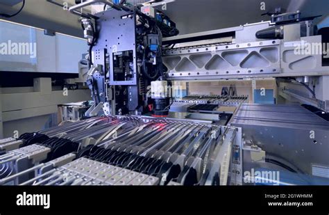
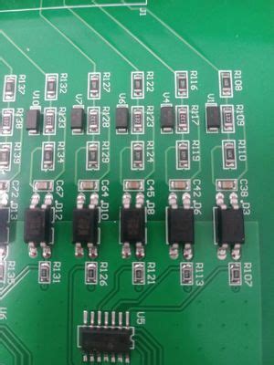
Precision placement of SMD components forms the cornerstone of high-yield PCB assembly processes. Modern pick-and-place systems achieve sub-10-micron accuracy through advanced vision alignment and servo-controlled nozzles, minimizing misalignment-induced defects. Engineers optimize PCBA outcomes by tailoring feeder configurations to component sizes—critical for handling ultra-miniaturized 0201 packages or large QFN ICs without compromising speed.
Tip: Regular calibration of placement equipment using certified fiducial markers reduces positional errors by up to 37% in mixed-technology boards.
Thermal management strategies during placement prevent premature solder paste drying, particularly when working with moisture-sensitive devices. Implementing dynamic Z-axis control adapts placement pressure for fragile components like ceramic capacitors, reducing mechanical stress risks. Recent studies show that pairing automated optical inspection (AOI) with real-time placement data analytics cuts rework rates by 19% in high-density SMD board assembly lines.
For multi-stage PCB assembly workflows, synchronizing placement speeds with upstream solder paste printing and downstream reflow processes prevents bottlenecks. A 2023 IPC benchmark report highlights that factories adopting AI-driven component sequencing improved throughput by 28% while maintaining 99.92% first-pass yield in PCBA operations. Process validation through design-of-experiments (DoE) methods further refines nozzle selection and vacuum parameters for diverse component portfolios.
Reflow Profiling Techniques for Reliable Assemblies
Effective reflow profiling is critical for ensuring robust solder joints in PCB assembly processes. Modern temperature-controlled ovens utilize multi-zone heating to manage thermal gradients, preventing component stress while activating solder paste optimally. By analyzing thermal profiles tailored to specific PCBA designs, manufacturers achieve precise control over peak temperatures and soak times, minimizing defects like tombstoning or cold solder joints.
Advanced systems now integrate real-time monitoring to adjust profiles dynamically, accounting for variations in board thickness or component density. For instance, ramp-to-spike profiles are increasingly used for lead-free solders, which require higher melting points without compromising adjacent components. Pairing these techniques with predictive modeling software allows engineers to simulate outcomes before production, reducing trial runs and material waste.
Transitioning from manual adjustments to data-driven profiling not only enhances yield but also aligns with automated inspection systems in downstream processes. This synergy ensures that PCB assembly lines maintain consistency across high-volume batches while meeting stringent reliability standards for industries like aerospace or medical devices.
Automated Inspection in SMD Board Production
Modern PCB assembly workflows increasingly rely on automated inspection systems to minimize defects and maintain high PCBA quality. Advanced optical inspection (AOI) and X-ray imaging technologies now enable real-time detection of issues like misaligned components, solder bridging, or insufficient paste volume. These systems analyze placement accuracy down to ±10 microns, ensuring compliance with tight tolerances required for high-density designs.
| Inspection Method | Key Capabilities | Defect Detection Rate |
|---|---|---|
| AOI Systems | 2D/3D component alignment, solder joint inspection | 98-99% |
| X-Ray Imaging | Hidden solder joints, BGA void analysis | 99.5% |
Integrated PCB assembly lines combine these tools with machine learning algorithms to refine process control feedback loops. For instance, AOI data can trigger automatic recalibration of pick-and-place machines, reducing human intervention. In PCBA environments handling miniaturized components (e.g., 0201 packages or micro-BGAs), automated electrical testing further validates functional performance before final packaging. This multi-layered approach reduces rework rates by up to 70% while maintaining traceability for compliance with IPC-A-610 standards. By synchronizing inspection data with production dashboards, manufacturers achieve predictive quality analytics, enabling proactive adjustments to soldering profiles or stencil designs.
Enhancing Efficiency with Precision SMD Assembly
Achieving high manufacturing yields in PCB assembly relies on optimizing precision at every stage of SMD component placement. Modern automated pick-and-place systems leverage vision-guided robotics to position components with micron-level accuracy, minimizing misalignment risks that lead to rework. By integrating real-time feedback loops, these systems dynamically adjust placement parameters based on PCBA design specifications, ensuring consistent adherence to tolerances even for ultra-fine-pitch components.
Critical to this process is the synchronization of component feeders, nozzle selection, and conveyor speed, which reduces idle time between placements. For example, dual-lane assembly lines enable simultaneous processing of multiple boards, doubling throughput without compromising placement quality. Advanced software algorithms further enhance efficiency by optimizing pick-up sequences and minimizing robotic arm travel distances.
Equally vital is maintaining strict environmental controls, as temperature and humidity fluctuations can affect solder paste viscosity and component behavior. Pairing precision placement with closed-loop reflow profiling creates a seamless workflow, where each stage of SMD board assembly reinforces the next. This systemic approach not only accelerates production but also reduces defects caused by manual interventions, ensuring that PCBA outputs meet rigorous reliability standards.
Solder Paste Application Best Practices
Effective solder paste application forms the foundation of high-quality PCB assembly, directly influencing joint integrity and electrical performance. Modern PCBA processes rely on precise stencil printing, where parameters such as aperture design, squeegee pressure, and snap-off distance must align with the thermal profile of subsequent reflow stages. Optimal solder paste viscosity ensures consistent deposition, minimizing voiding or bridging defects. For fine-pitch components, laser-cut stainless steel stencils with electropolished walls enhance paste release accuracy by up to 98%, particularly critical for 0.4mm-pitch ICs or μBGA packages.
Automated vision systems now integrate real-time height mapping to compensate for board warpage, adjusting print pressure dynamically. Post-application inspection via 3D SPI (Solder Paste Inspection) identifies deviations in volume, alignment, or shape before reflow, reducing rework costs by 30–40%. Best practices also emphasize environmental controls: maintaining 25±3°C and 40–60% RH prevents paste drying and ensures stable rheology.
In high-mix PCB assembly environments, no-clean formulations with Type 4 or 5 powder sizes balance slump resistance and reflow activity. For PCBA involving mixed alloys, sequential printing or dual-lane systems prevent cross-contamination. Process engineers increasingly adopt machine learning algorithms to predict paste behavior under varying line conditions, further tightening CpK values for critical applications.
Reducing Defects in SMD Manufacturing Processes
Defect reduction in SMD board assembly requires a systematic approach to identify and address root causes across the PCBA workflow. Common issues such as solder bridging, component misalignment, and insufficient solder joints often stem from inconsistencies in solder paste application or thermal imbalances during reflow. Implementing statistical process control (SPC) tools helps monitor critical parameters like stencil aperture alignment and paste viscosity, ensuring uniformity in PCB assembly stages.
Advanced automated optical inspection (AOI) systems now integrate machine learning algorithms to detect micron-level deviations in component placement, reducing false positives by up to 40% compared to traditional methods. For high-reliability PCBA, nitrogen-assisted reflow ovens minimize oxidation, while real-time temperature profiling ensures optimal thermal gradients for diverse component sizes. Additionally, adopting closed-loop feedback mechanisms between pick-and-place machines and inspection systems enables immediate corrections, slashing defect rates by 25–30% in high-volume production.
Material selection also plays a pivotal role—low-residue solder pastes and moisture-resistant substrates mitigate risks of electrochemical migration or delamination. By harmonizing these strategies, manufacturers achieve tighter process windows, directly enhancing yield and long-term reliability in SMD manufacturing.
Advanced Technologies for High-Yield SMD Assembly
Modern PCB assembly processes leverage advanced technologies to address challenges in SMD board assembly, particularly in achieving consistent manufacturing yields. Innovations such as 3D solder paste inspection (SPI) systems enable real-time monitoring of deposition accuracy, reducing defects caused by insufficient or excess solder volume. For PCBA workflows, adaptive machine learning algorithms now optimize component placement paths, minimizing misalignment risks while accelerating throughput. High-precision vision-guided robotics further enhance placement accuracy, especially for ultra-fine-pitch components below 0.4mm.
Thermal profiling advancements, including predictive reflow oven control, ensure uniform heat distribution across complex boards, mitigating tombstoning or voiding defects. Additionally, inline automated optical inspection (AOI) systems equipped with multispectral imaging detect microfractures or soldering anomalies at speeds exceeding 20,000 components per hour. Integrating these technologies into unified PCB assembly platforms allows manufacturers to maintain traceability, correlate process data, and implement corrective actions in near real-time. By combining precision tooling with data-driven analytics, PCBA providers achieve yield improvements exceeding 98%, even for high-density designs requiring 01005-sized components or advanced packaging formats like QFN and BGA.
Boosting Reliability Through Process Optimization
Effective PCB assembly reliability stems from systematic process optimization that addresses both micro-level component interactions and macro-level production variables. By implementing statistical process control (SPC) methodologies, manufacturers can identify deviations in critical parameters such as reflow oven temperature gradients, pick-and-place nozzle pressure, and stencil alignment tolerances. Real-time monitoring systems integrated into PCBA lines enable rapid adjustments to solder paste deposition thickness or component placement accuracy, minimizing latent defects like tombstoning or cold joints.
A key strategy involves optimizing the feedback loop between automated optical inspection (AOI) systems and assembly equipment. For instance, thermal profiling data from post-reflow inspections can refine oven settings to maintain peak soldering consistency across batch variations. Additionally, standardizing cleaning protocols for solder paste residues prevents electrochemical migration—a common failure mode in high-density PCB assembly. When combined with machine learning algorithms that predict equipment wear patterns, these optimizations create a self-correcting production environment, elevating first-pass yield rates while reducing warranty returns by up to 22% in field-tested implementations.
Conclusion
In modern electronics manufacturing, achieving high yields in SMD board assembly demands a systematic integration of precision processes and intelligent quality control. By leveraging advancements in PCB assembly workflows—such as adaptive component placement algorithms and dynamic reflow profiling—manufacturers can significantly reduce defects while scaling production efficiency. The role of automated optical inspection (AOI) systems in PCBA lines cannot be overstated, as they enable real-time defect detection and correction, ensuring compliance with stringent reliability standards.
Furthermore, the adoption of machine learning-driven solder paste inspection and predictive maintenance protocols underscores the industry’s shift toward data-centric methodologies. These innovations not only optimize material utilization but also extend equipment longevity, directly contributing to cost-effective manufacturing. As SMD technologies continue to evolve, aligning process parameters with emerging component miniaturization trends remains critical. By prioritizing closed-loop feedback mechanisms and cross-functional process validation, manufacturers can sustain high yields while adapting to the accelerating demands of next-generation electronics. The convergence of precision engineering and smart automation ultimately defines the future of high-reliability PCB assembly.
FAQs
What are the primary benefits of advanced SMD assembly methods?
Advanced SMD board assembly techniques improve manufacturing yield by optimizing PCB assembly processes like precision component placement and reflow profiling. These methods reduce human error and ensure consistent solder joint quality, directly enhancing product reliability.
How does PCBA differ from traditional PCB manufacturing?
While PCB assembly focuses on mounting components onto a bare board, PCBA (Printed Circuit Board Assembly) encompasses the entire process, including soldering, testing, and inspection. Advanced PCBA integrates automated systems to achieve higher accuracy and throughput.
What role does reflow profiling play in SMD assembly?
Reflow profiling ensures optimal temperature distribution during soldering, preventing defects like tombstoning or cold joints. By fine-tuning thermal curves, manufacturers achieve reliable PCB assembly outcomes, especially for heat-sensitive components.
Why is automated inspection critical in modern SMD production?
Automated optical inspection (AOI) and X-ray systems identify microscopic defects—such as misaligned components or insufficient solder—that manual checks might miss. This step is vital for maintaining high-yield PCBA workflows.
What common defects occur in SMD manufacturing, and how are they mitigated?
Common issues include solder bridging and component misalignment. These are addressed through precision stencil design for solder paste application and real-time calibration of pick-and-place machines in PCB assembly lines.
How does precision placement enhance manufacturing efficiency?
High-speed placers with vision systems position components within microns of accuracy, reducing rework and material waste. This precision is foundational for scalable PCBA solutions in high-volume production.
What should manufacturers prioritize when selecting a PCBA service provider?
Look for expertise in thermal management, process validation protocols, and integration of inspection technologies. Providers offering end-to-end PCB assembly solutions typically deliver better yield consistency and faster turnaround.
Optimize Your SMD Assembly Today
Ready to elevate your PCBA quality and yield? Click here to explore tailored PCB assembly solutions designed for precision and reliability.